July 2005
rev 1.0
ASM3P623S00A/B/C/D/E/F
Spread Spectrum Frequency Generation
The clocks in digital systems are typically square waves
with a 50% duty cycle and as frequencies increase the
edge rates also get faster. Analysis shows that a square
wave is composed of fundamental frequency and
harmonics. The fundamental frequency and harmonics
generate the energy peaks that become the source of
EMI. Regulatory agencies test electronic equipment by
measuring the amount of peak energy radiated from the
equipment. In fact, the peak level allowed decreases as
the frequency increases. The standard methods of
reducing EMI are to use shielding, filtering, multi-layer
PCBs etc. These methods are expensive. Spread
spectrum clocking reduces the peak energy by reducing
the Q factor of the clock. This is done by slowly
modulating the clock frequency. The ASM3P623S00X
uses the center modulation spread spectrum technique in
which the modulated output frequency varies above and
below the reference frequency with
a
specified
modulation rate. With center modulation, the average
frequency is the same as the unmodulated frequency and
there is no performance degradation
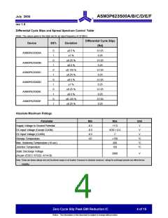
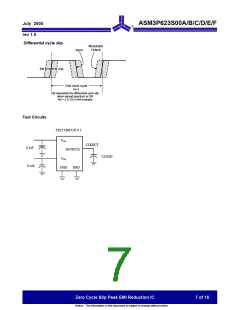
Cycle Slip
Cycle slip occurs when the output clock edge
‘wanders’ away from the corresponding input clock
edge. There are two types of cycle slips – a Differential
cycle slip and an Integral cycle slip. The differential
cycle slip is caused due the clock edge variation over
one modulation cycle. It is defined by the maximum
amount of ‘wander’ the clock edge will have within one
modulation cycle. Integral cycle slip occurs due to the
accumulation of the cycle slip over successive modulation
cycles. In ASM3P623S00A/B/C/D/E/F the differential cycle
slip is within the value mentioned in the “Differential Cycle
Slip and Spread Spectrum Control Table” and the Integral
Cycle Slip is ‘Zero’.
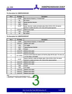
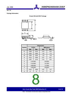
Pin Configuration
NC
8
CLKIN
NC
1
VDD
7
6
5
2
3
ASM3P623S00A/B/C
CLKOUT
SSON
SS%
GND
4
1
CLKOUT8
CLKOUT7
CLKOUT6
VDD
CLKIN
16
15
14
13
12
11
10
9
2
3
CLKOUT1
VDD
SS%
4
ASM3P623S00 D/E/F
GND
GND
5
6
7
CLKOUT5
CLKOUT4
SSON
CLKOUT2
CLKOUT3
DLY CNTRL
8
Zero Cycle Slip Peak EMI Reduction IC
2 of 16
Notice: The information in this document is subject to change without notice.

 PULSECORE [ PulseCore Semiconductor ]