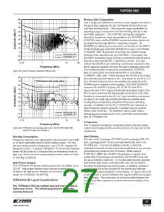
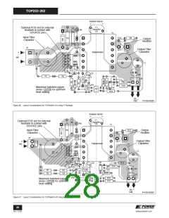
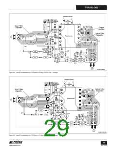
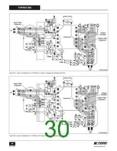
TOP252-262
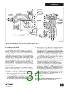
Isolation Barrier
Y1-
Capacitor
C7
C6
R12
T1
C16
R7
Input Filter
Capacitor
C4
R6
VR1
D8
J1
HS2
+
HV
-
Output
Transformer
Rectifier
D5
R22
JP1
X
F
D
Output Filter
Capacitor
C17
S
Y
C
C8
U1
R8
L3
C9
C10
C18
D6
U4
HS1
C19
J2
R10
C21
R20
VR2
R9
R17
R13
Note: Components U1, R8, C8, C9 and R22
are under heat sink HS1.
U2
JP2
R15
R21
-
+
DC
Out
PI-5216-091508
Figure 50c. Layout Considerations for TOPSwitch-HX Using L-Package and Operating at 132 kHz.
2. Maximum drain current – At maximum ambient temperature,
maximum input voltage and maximum output load, verify
drain current waveforms at start-up for any signs of trans-
former saturation and excessive leading edge current spikes.
TOPSwitch-HX has a leading edge blanking time of 220 ns
to prevent premature termination of the ON-cycle. Verify that
the leading edge current spike is below the allowed current
limit envelope (see Figure 53) for the drain current waveform
at the end of the 220 ns blanking period.
Quick Design Checklist
In order to reduce the no-load input power of TOPSwitch-HX
designs, the V-pin (or M-pin for P Package) operates at very
low current. This requires careful layout considerations when
designing the PCB to avoid noise coupling. Traces and
components connected to the V-pin should not be adjacent to
any traces carrying switching currents. These include the drain,
clamp network, bias winding return or power traces from other
converters. If the line sensing features are used, then the sense
resistors must be placed within 10 mm of the V-pin to minimize
the V pin node area. The DC bus should then be routed to the
line sense resistors. Note that external capacitance must not
be connected to the V-pin as this may cause misoperaton of the
V pin related functions.
3. Thermal check – At maximum output power, both minimum
and maximum voltage and ambient temperature; verify that
temperature specifications are not exceeded for
TOPSwitch-HX, transformer, output diodes and output
capacitors. Enough thermal margin should be allowed for
the part-to-part variation of the RDS(ON) of TOPSwitch-HX, as
specified in the data sheet. The margin required can either
be calculated from the values in the parameter table or it can
be accounted for by connecting an external resistance in
series with the DRAIN pin and attached to the same heat
sink, having a resistance value that is equal to the difference
between the measured RDS(ON) of the device under test and
the worst case maximum specification.
As with any power supply design, all TOPSwitch-HX designs
should be verified on the bench to make sure that components
specifications are not exceeded under worst-case conditions.
The following minimum set of tests is strongly recommended:
1. Maximum drain voltage – Verify that peak VDS does not
exceed 675 V at highest input voltage and maximum
overload output power. Maximum overload output power
occurs when the output is overloaded to a level just before
the power supply goes into auto-restart (loss of regulation).
Design Tools
Up-to-date information on design tools can be found at the
Power Integrations website: www.powerint.com
31
www.powerint.com
Rev. F 01/09

 POWERINT [ Power Integrations ]