RELEASED
PM7350 S/UNI DUPLEX
DATA SHEET
PMC-1980581
ISSUE 8
DUAL SERIAL LINK PHY MULTIPLEXER
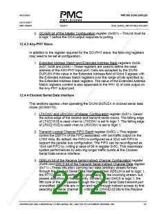
Serial Indirect Channel (0x68)Select or the Transmit Serial Indirect
Channel Select (0x70). Writing a logic 0 to CRWB of the same registers
triggers an indirect write operation. Writing a logic 1 to CRWB of the same
registers triggers an indirect read operation.
4. ALIGN bit of the Transmit Serial Alignment Control register (0x74) – This
bit allows ATM/DATA octet alignment to frame boundaries based on
recognizing gaps in the transmit serial clock. When this bit is set to logic 1,
the ATM /Data octets are aligned to the inferred frame alignment, with the
most significant bit output first during the clock gap on all sixteen transmit
channels.
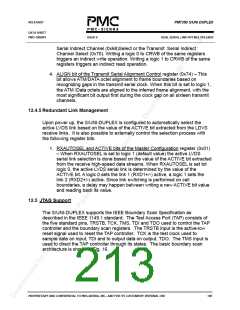
12.4.5 Redundant Link Management
Upon power up, the S/UNI-DUPLEX is configured to automatically select the
active LVDS link based on the value of the ACTIVE bit extracted from the LDVS
receive links. It is also possible to externally control the selection process with
the following register bits.
1. RXAUTOSEL and ACTIVE bits of the Master Configuration register (0x01)
– When RXAUTOSEL is set to logic 1 (default value) the active LVDS
serial link selection is done based on the value of the ACTIVE bit extracted
from the receive high-speed data streams. When RXAUTOSEL is set tot
logic 0, the active LVDS serial link is determined by the value of the
ACTIVE bit. A logic 0 sets the link 1 (RXD1+/-) active, a logic 1 sets the
link 2 (RXD2+/-) active. Since link switching is performed on cell
boundaries, a delay may happen between writing a new ACTIVE bit value
and reading back its value.
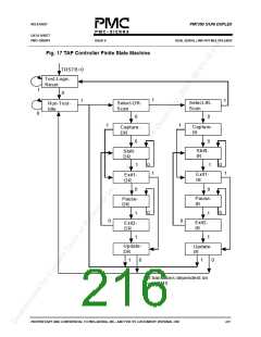
12.5 JTAG Support
The S/UNI-DUPLEX supports the IEEE Boundary Scan Specification as
described in the IEEE 1149.1 standard. The Test Access Port (TAP) consists of
the five standard pins, TRSTB, TCK, TMS, TDI and TDO used to control the TAP
controller and the boundary scan registers. The TRSTB input is the active-low
reset signal used to reset the TAP controller. TCK is the test clock used to
sample data on input, TDI and to output data on output, TDO. The TMS input is
used to direct the TAP controller through its states. The basic boundary scan
architecture is shown in Fig. 16.
PROPRIETARY AND CONFIDENTIAL TO PMC-SIERRA, INC., AND FOR ITS CUSTOMERS’ INTERNAL USE
198

 PMC [ PMC-SIERRA, INC ]