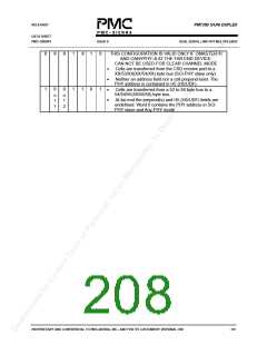
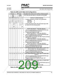
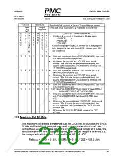
RELEASED
PM7350 S/UNI DUPLEX
DATA SHEET
PMC-1980581
ISSUE 8
DUAL SERIAL LINK PHY MULTIPLEXER
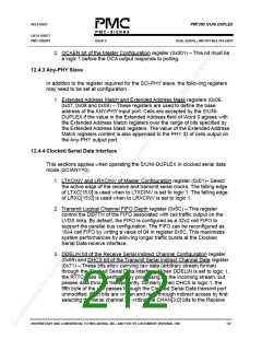
2. OCAEN bit of the Master Configuration register (0x001) – This bit must be
a logic 1 before the OCA output responds to polling.
12.4.3 Any-PHY Slave
In addition to the register required for the SCI-PHY slave, the following registers
may need to be set at configuration
1. Extended Address Match and Extended Address Mask registers (0x06,
0x07, 0x08 and 0x09) – These registers are used to define the base
address of the ANY-PHY input port. Cells are accepted by the S/UNI-
DUPLEX if the value in the Extended Address field of Word 0 agrees with
the Extended Address Match registers over the range of bits specified by
the Extended Address Mask registers. The value of the Extended Address
Match registers content is also appended to the PHY ID of cells output on
the Any-PHY output port.
12.4.4 Clocked Serial Data Interface
This sections applies when operating the S/UNI-DUPLEX in clocked serial data
mode (SCIANY=0).
1. LTXCINV and LRXCINV of Master Configuration register (0x01)– Select
the active edge of the receive and transmit serial clocks. The falling edge
of LTXC[15:0] is used when to LTXCINV is set to logic 1. The falling edge
of LRXC[15:0] is used when to LRXCINV is set to logic 1.
2. Transmit Logical Channel FIFO Depth register (0x5C) – This register
control the DEPTH of the FIFO associated with cell traffic output on the
LVDS links. By default, the FIFO is configured as a 32x2 cell FIFO to
support the parallel bus configuration. The FIFO can be reconfigured as
16x4 cell FIFO by writing a value of 04 in register 0x5C. This maximizes
system performances by allowing longer traffic bursts at the Clocked
Serial Data receive interface.
3. DDELIN bit of the Receive Serial Indirect Channel Configuration register
(0x69) and DHCS bit of the Transmit Serial Indirect Channel Data register
(0x71) – These bits allow carrying raw data (arbitrary stream format)
through the Clocked Serial Data interface. When DDELIN is set to logic 1,
the RTTC does not perform any processing on the incoming stream, but
passes data through transparently. Similarly when DHCS is logic 1, the
fifth byte of the cell passes through the Clocked Serial Data transmit port
unmodified. Both bits are written and read through indirect access by first
selecting the serial channel by writing the CHAN[3:0] bits to the Receive
PROPRIETARY AND CONFIDENTIAL TO PMC-SIERRA, INC., AND FOR ITS CUSTOMERS’ INTERNAL USE
197

 PMC [ PMC-SIERRA, INC ]