RELEASED
PM7350 S/UNI DUPLEX
DATA SHEET
PMC-1980581
ISSUE 8
DUAL SERIAL LINK PHY MULTIPLEXER
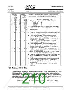
Ratiomin = 52/61 = 85.2%, CellBRmin = 85.2% * 200 = 170.5Mb/s
In addition to the LVDS stream capacity, the total Clocked Serial Data interface
throughput is limited by the aggregate number of clock actives edges of all lines
in each direction, independently of the idle and discarded cells. The
instantaneous aggregate bit rate of all clocked serial data receive lines (including
idle and discarded cells) has to be equal or less than the LVDS bit rate.
12.4 Minimum Programming
Besides the bus configuration described in the previous section, very little
configuration is required to make the part function. The S/UNI-DUPLEX can
operate in SCI-PHY/Utopia master mode or in Clocked Serial Data without
external intervention. In addition to the registers described below, the following bit
is commonly modified:
1. MINTE bit of the Master Configuration register (0x001) – This bit must be
logic 1 to enable interrupt servicing. If MINTE is logic 0, the INTB output
will be unconditionally high-impedance. Note that individual interrupt
sources must enabled in addition to setting MINTE.
The following three sections apply when operating the S/UNI-DUPLEX in parallel
bus mode (SCIANY=1).
12.4.1 SCI-PHY/Utopia Master Mode
Although the default setting allows cell traffic to go, system performances may be
improved by modifying the following registers.
1. PHYID[5:0] bits SCI-PHY/Any-PHY Input Configuration 2 and SCI-
PHY/Any-PHY Output Polling Range registers (0x0D, 0x15) – These bits
are used to define the polling range of the SCI/PHY/Any-PHY input and
output interface.
2. Input Cell Available Enable registers (0x10, 0x11, 0x12 and 0x13) – These
registers can be used to dynamically remove PHYs from in the input port
polling list. Setting a bit of these registers to logic 0 removes the
corresponding PHY ID from the polling list.
12.4.2 SCI-PHY Slave
1. Output Address Match register (0x0A) – This register is used to set the
proxy PHY ID for selection and transfer of cells on the SCI-PHY/Any-PHY
output interface.
PROPRIETARY AND CONFIDENTIAL TO PMC-SIERRA, INC., AND FOR ITS CUSTOMERS’ INTERNAL USE
196

 PMC [ PMC-SIERRA, INC ]