PM6341 E1XC
DATA SHEET
PMC-910419
ISSUE 8
E1 FRAMER/TRANSCEIVER
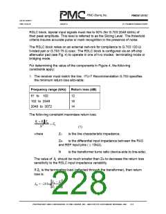
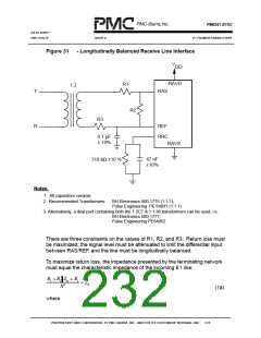
Zo =
R1(R2 + R3||Zin)
where Zo = line characteristic
impedance.
2
N (R1+ R2+ R3||Zin)
The value of R3 should be much smaller than 10 kΩ to decrease the return
loss sensitivity to the RSLC input impedance variability.
If Z is the reflected load, then return loss is
L
L = -20log|(Z - Zo)/(Z + Zo)|
R
L
L
Provided tightly toleranced components are used, the ITU-T return loss
specifications are easily met.
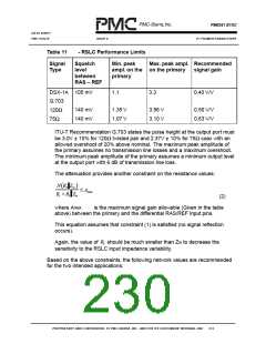
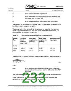
2. The signal should be attenuated to a level compatible with the slicer.
The maximum potential between the RAS and REF pins must be less than
1.96V to prevent internal circuitry from saturating.
The minimum peak amplitude between the RAS and REF pins must be large
enough to ensure reliable operation; bit errors may occur if the amplitude is
below 213 mV. If the amplitude drops below 105 mV for a 67% slicing
threshold and 140 mV for a 50% slicing threshold, the RSLC outputs are
forced to logic 0 and a squelch alarm is raised. The squelching prevents the
slicing of noise on an idle transmission line. (The SQ status bit goes high
whenever the RSLC block is squelching. The block can be configured to
generate an interrupt whenever the SQ status bit goes high.)
The RSLC was not designed for line lengths greater than 1000 ft. Although it
can handle considerable flat loss, pulse spreading and inter-symbol
interference results in unreliable operation for long line lengths.
With the above limits in mind, it is recommended the attenuation shall be
such that the differential signal level across RAS/REF be 1.96 V peak for the
maximum expected signal level at the primary. The following table
summarizes the limits:
PROPRIETARY AND CONFIDENTIAL TO PMC-SIERRA, INC., AND FOR ITS CUSTOMERS’ INTERNAL USE
213

 PMC [ PMC-SIERRA, INC ]