PM6341 E1XC
DATA SHEET
PMC-910419
ISSUE 8
E1 FRAMER/TRANSCEIVER
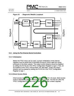
14.5.3 Indirect Access Mode
Indirect access mode is selected by setting the IND bit in the TPSC Configuration
Register to logic 1. When using the indirect access mode, the status of the
BUSY indication bit should be polled to determine the status of the
microprocessor access: when the BUSY bit is logic 1, the TPSC is processing an
access request; when the BUSY bit is logic 0, the TPSC has completed the
request.
The indirect write programming sequence for the TPSC is as follows:
1. Check that the BUSY bit in the TPSC µP Access Status Register is logic 0.
2. Write the timeslot data to the TPSC Timeslot Indirect Data Buffer register.
3. Write RWB=0 and the timeslot address to the TPSC Timeslot Indirect
Address/Control Register.
4. Poll the BUSY bit until it goes to logic 0. The BUSY bit will go to logic 1
immediately after step 3 and remain at logic 1 until the request is complete.
5. If there is more data to be written, go back to step 1.
The indirect read programming sequence for the TPSC is as follows:
1. Check that the BUSY bit in the TPSC µP Access Status Register is logic 0.
2. Write RWB=1 and the timeslot address to the TPSC Timeslot Indirect
Address/Control Register.
3. Poll the BUSY bit, waiting until it goes to a logic 0. The BUSY bit will go to
logic 1 immediately after step 2 and remain at logic 1 until the request is
complete.
4. Read the requested timeslot data from the TPSC Timeslot Indirect Data
Buffer register.
5. If there is more data to be read, go back to step 1.
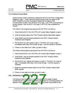
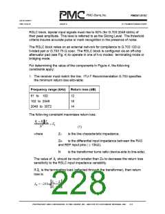
14.6 Interfacing to the Analog Pulse Slicer
The Receive Data Slicer (RSLC) block provides the first stage of signal
conditioning for a G.703 2048 kbit/s serial data stream by converting bipolar line
signals to dual rail RZ pulses. Before an RZ output pulse is generated by the
PROPRIETARY AND CONFIDENTIAL TO PMC-SIERRA, INC., AND FOR ITS CUSTOMERS’ INTERNAL USE
211

 PMC [ PMC-SIERRA, INC ]