PM6341 E1XC
DATA SHEET
PMC-910419
ISSUE 8
E1 FRAMER/TRANSCEIVER
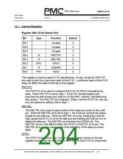
testing. When IOTST is a logic 1, all blocks are held in test mode and the
microprocessor may write to a block's test mode 0 registers to manipulate the
outputs of the block and consequently the device outputs (refer to the "Test
Mode 0 Details" in this section).
HIZIO, HIZDATA:
The HIZIO and HIZDATA bits control the tristate modes of the E1XC . While
the HIZIO bit is a logic 1, all output pins of the E1XC except the data bus are
held in a high-impedance state. The microprocessor interface is still active.
While the HIZDATA bit is a logic 1, the data bus is also held in a high-
impedance state which inhibits microprocessor read cycles.
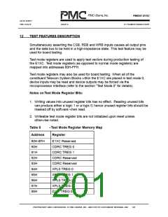
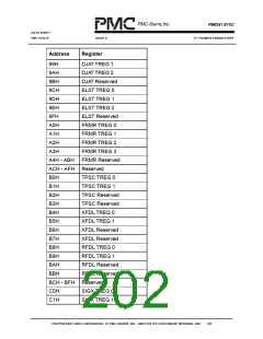
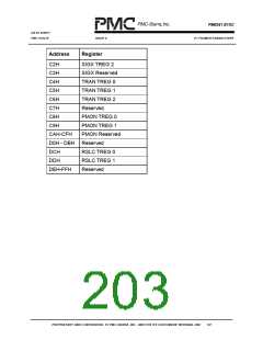
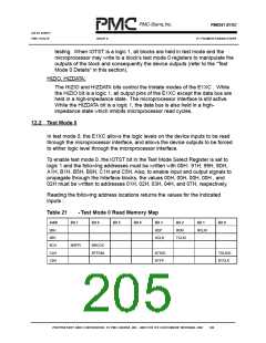
12.2 Test Mode 0
In test mode 0, the E1XC allows the logic levels on the device inputs to be read
through the microprocessor interface, and allows the device outputs to be forced
to either logic level through the microprocessor interface.
To enable test mode 0, the IOTST bit in the Test Mode Select Register is set to
logic 1 and the following addresses must be written with 00H: 91H, 99H, 9DH,
A1H, B1H, B5H, B9H, C1H and C5H. Also, to enable input and output signals to
propagate through the Interface blocks, the values 00H, 00H, 00H, 00H , and
02H must be written to addresses 01H, 02H, 03H, 04H, and 07H, respectively.
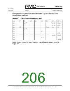
Reading the following address locations returns the values for the indicated
inputs :
Table 21
-Test Mode 0 Read Memory Map
Addr
90H
98H
9CH
C4H
C6H
Bit 7
Bit 6
Bit 5
Bit 4
Bit 3
RDP
XCLK
Bit 2
RDN
Bit 1
Bit 0
RCLKI
TCLKI
BRFPI
BRCCK
BTPCM
BTSIG
BTFP
TDLSIG
BTCLK
PROPRIETARY AND CONFIDENTIAL TO PMC-SIERRA, INC., AND FOR ITS CUSTOMERS’ INTERNAL USE
189

 PMC [ PMC-SIERRA, INC ]