PM6341 E1XC
DATA SHEET
PMC-910419
ISSUE 8
E1 FRAMER/TRANSCEIVER
13
TIMING DIAGRAMS
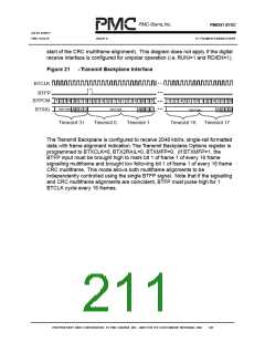
Figure 13
-TS16Transmit Datalink Interface
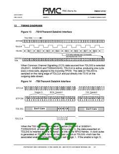
Time Slots
BTPCM 15 16 17 18 19 20 21 22 23 24 25 26 27 28 29 30 31
0
1
2
3
4
5
6
7
8
9
10 11 12 13 14 15 16 17
TDLCLK
TDLSIG
Bit 1
Bit 2
Bit 3
Bit 4
Bit 5
Bit 6
Bit 7
Bit 8
CCS data collected over 32 timeslots
and inserted into TS16
TDP/TDD
TDN
14 15 16 17 18 19 20 21 22 23 24 25 26 27 28 29 30 31
0
1
2
3
4
5
6
7
8
9
10 11 12 13 14 15 16
When Common Channel Signalling (CCS) data sourced from TDLSIG is selected
(DLEN=1, SIGEN=0 and TXDMASIG=0), TDLCLK is active, producing one cycle
every 4 time slots, aligned to the incoming TPCM. The data on TDLSIG is
sampled on the rising edge of TDLCLK and put directly into TS16 on the
outgoing data stream.
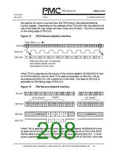
Figure 14
-TS0Transmit Datalink Interface
BTCLK
Timeslot 31
NFAS, Timeslot 0
FAS, Timeslot 0
7 8 1 2 3 4 5 6 7 8 1 2 3 4 5 6 7 8 1 2 3 4 5
7 8 1 2 3 4 5 6 7 8 1 2
BTPCM
Don't Care
4 5 6 7 8
TDLSIG
TDLCLK
Don't Care
When the TS0 maintenance datalink is active (DLEN=0 or SIGEN=1,
TXDMASIG=0, at least one TXSAxEN bit is a logic 1), the data presented on
TDLSIG is inserted into the National Use bits of the NFAS frames. A clock pulse
is generated on TDLCLK for each National Use bit on TDLSIG which has the
associated enable (TXSAxEN, x=4 to 8) set to logic 1. If the enable is logic 0,
PROPRIETARY AND CONFIDENTIAL TO PMC-SIERRA, INC., AND FOR ITS CUSTOMERS’ INTERNAL USE
191

 PMC [ PMC-SIERRA, INC ]