PM6341 E1XC
DATA SHEET
PMC-910419
ISSUE 8
E1 FRAMER/TRANSCEIVER
12
TEST FEATURES DESCRIPTION
Simultaneously asserting the CSB, RDB and WRB inputs causes all output pins
and the data bus to be held in a high-impedance state. This test feature may be
used for board testing.
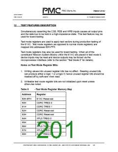
Test mode registers are used to apply test vectors during production testing of
the E1XC. Test mode registers (as opposed to normal mode registers) are
mapped into addresses 80H-FFH.
Test mode registers may also be used for board testing. When all of the
constituent Telecom System Blocks within the E1XC are placed in test mode 0,
device inputs may be read and device outputs may be forced via the
microprocessor interface (refer to the section "Test Mode 0" for details).
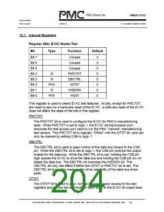
Notes onTest Mode Register Bits:
1. Writing values into unused register bits has no effect. Reading unused bits
can produce either a logic 1 or a logic 0; hence unused register bits should be
masked off by software when read.
2. Writeable test mode register bits are not initialized upon reset unless
otherwise noted.
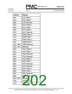
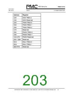
Table 9
-Test Mode Register Memory Map
Register
Address
80H-8FH
90H
E1XC Reserved
CDRC TREG 0
CDRC TREG 1
CDRC Reserved
CDRC Reserved
XPLS TREG 0
XPLS TREG 1
XPLS TREG 2
XPLS TREG 3
DJAT TREG 0
91H
92H
93H
94H
95H
96H
97H
98H
PROPRIETARY AND CONFIDENTIAL TO PMC-SIERRA, INC., AND FOR ITS CUSTOMERS’ INTERNAL USE
185

 PMC [ PMC-SIERRA, INC ]