S/UNI®-8x155 ASSP Telecom Standard Product Data Sheet
Released
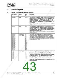
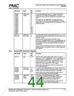
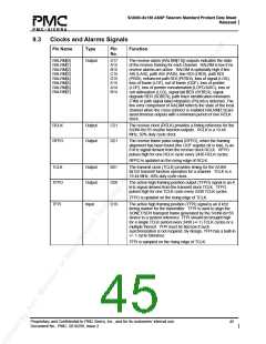
9.4
Section and Line Status DCC Signals
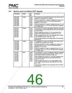
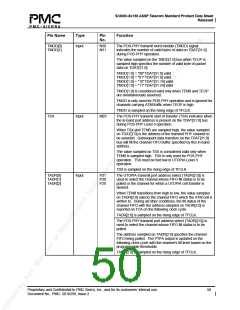
Pin Name
Type
Pin
Function
No.
RDCLK[0]
RDCLK[1]
RDCLK[2]
RDCLK[3]
RDCLK[4]
RDCLK[5]
RDCLK[6]
RDCLK[7]
Output
AG31
AH30
AK28
AL27
AK26
AL25
AK24
AK23
The receive DCC clocks (RDCLK[7:0]) are the clocks used to
update the associated RDCC outputs.
When the channel DCC output is configured for section DCC,
the associated RDCLK is a 192 kHz clock generated by
gapping a 216 kHz clock.
When the channel DCC output is configured for line DCC, the
associated RDCLK is a 576 kHz clock generated by gapping
a 2.16 MHz clock.
RDCC[0]
RDCC[1]
RDCC[2]
RDCC[3]
RDCC[4]
RDCC[5]
RDCC[6]
RDCC[7]
Output
AF29
AG28
AH27
AJ26
AG25
AH24
AJ24
AG22
The receive DCC (RDCC[7:0]) signals contain the serial data
communication channels extracted from the incoming stream
of each channel.
When configured for section DCC, the associated RDCC
output is the extracted section DCC bytes (D1, D2, D3).
When configured for line DCC, the associated RDCC output
is the extracted line DCC bytes (D4 - D12).
RDCC[7:0] are updated on the falling edge of the associated
RDCLK[7:0].
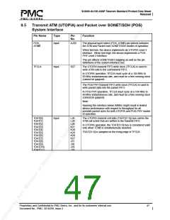
TDCLK[0]
TDCLK[1]
TDCLK[2]
TDCLK[3]
TDCLK[4]
TDCLK[5]
TDCLK[6]
TDCLK[7]
Output
Input
AF28
AG29
AJ27
AH26
AH25
AG24
AG23
AJ23
The transmit DCC clocks (TDCLK[7:0]) are the clocks used
to sample the associated TDCC inputs.
When the channel DCC input is configured for section DCC,
the associated TDCLK is a 192 kHz clock generated by
gapping a 216 kHz clock.
When the channel DCC input is configured for line DCC, the
associated TDCLK is a 576 kHz clock generated by gapping
a 2.16 MHz clock.
The transmit DCC (TDCC[7:0]) signals contain the serial data
communication channels of each channel. When not used,
these inputs should be connected to logic zero.
When configured for section DCC, the value sampled on the
TDCC input is inserted into the associated section DCC
bytes (D1, D2, D3).
When configured for line DCC, the value sampled on the
TDCC input is inserted into the associated line DCC bytes
(D4 – D12).
TDCC[0]
TDCC[1]
TDCC[2]
TDCC[3]
TDCC[4]
TDCC[5]
TDCC[6]
TDCC[7]
AG30
AF27
AG26
AK27
AJ25
AK25
AL24
AH23
TDCC[7:0] are sampled on the rising edge of the associated
TDCLK[7:0].
Proprietary and Confidential to PMC-Sierra, Inc., and for its customers’ internal use.
Document No.: PMC- 2010299, Issue 2
46

 PMC [ PMC-SIERRA, INC ]