S/UNI®-8x155 ASSP Telecom Standard Product Data Sheet
Released
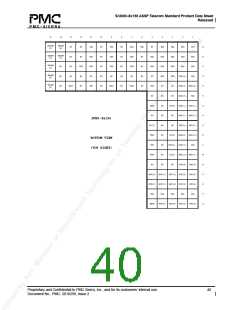
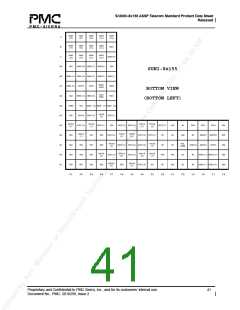
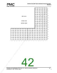
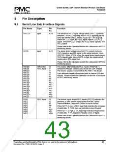
Pin Name
Type
Pin
No.
Function
TXD[0]+
TXD[0]-
TXD[1]+
TXD[1]-
TXD[2]+
TXD[2]-
TXD[3]+
TXD[3]-
TXD[4]+
TXD[4]-
TXD[5]+
TXD[5]-
TXD[6]+
TXD[6]-
TXD[7]+
TXD[7]-
Differential
Output
D2
The transmit differential data PECL outputs (TXD[7:0]+/)
contain the 155.52 Mbit/s transmit stream. The TXD+/-
outputs are driven using the synthesized clock from the CSU-
622.
The TXD[7:0]+/- are differential TLL outputs which are
converted to PECL levels using external passive networks.
Please refer to the Operation section for a discussion of PECL
interfacing issues.
E2
G2
G1
J2
J1
L2
L3
Y2
Y1
AB1
AB2
AD1
AD2
AF2
AG1
REFCLK+
Differential
PECL Input
V1
The differential reference clock inputs (REFCLK+/-) is a 77.76
MHz reference clock for both the clock recovery and the clock
synthesis circuits.
REFCLK-
V2
When the WAN Synchronization controller is used,
REFCLK+/- is supplied using a VCXO. In that application, the
serial transmit direction can be externally looped timed to the
line receiver in order to meet wander transfer and holdover
requirements.
Please refer to the Operation section for a discussion of PECL
interfacing issues and reference clocks. For jitter requirement
see Table 30.
9.2 Serial APS Interface Signals
Pin Name
Type
Pin
Function
No.
APECLV
Input
AJ18
The APS PECL signal voltage select (APECLV) selects
between 3.3V PECL signaling and 5V PECL signaling for the
APS (APSI[1:0]+/-) and REFCLK+/- PECL inputs. When
APECLV is low, the APSI[1:0]+/- and REFCLK+/- PECL
inputs expect a 5V PECL signal. When APECLV is high,
these PECL inputs expect a 3.3V PECL signal.
Please refer to the Operation section for a discussion of
PECL interfacing issues.
APSI[0]+
APSI[0]-
APSI[1]+
APSI[1]-
Differential
PECL Input
A17
B17
A18
B18
The receive APS differential data PECL inputs (APSI[1:0]+/-)
contain the NRZ bit serial APS stream for each channel. The
receive clock is recovered from the APS+/- bit stream.
Please refer to the Operation section for a discussion of
PECL interfacing issues and APS functionality.
APSO[0]+
APSO[0]-
APSO[1]+
APSO[1]-
Differential
PECL
AK17
AL17
AK18
AL18
The transmit APS differential data PECL outputs
(APSO[1:0]+/-) contain the 622.08 Mbit/s transmit APS
stream. The APSO+/- outputs are driven using the
synthesized clock from the clock synthesis unit.
Output
Please refer to the Operation section for a discussion of
PECL interfacing issues and APS functionality.
Proprietary and Confidential to PMC-Sierra, Inc., and for its customers’ internal use.
Document No.: PMC- 2010299, Issue 2
44

 PMC [ PMC-SIERRA, INC ]