Philips Semiconductors
Preliminary specification
Fault-tolerant CAN transceiver
TJA1054
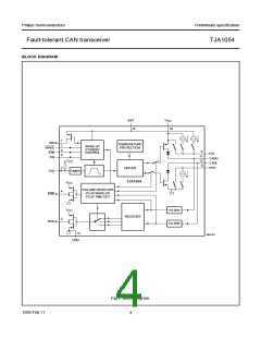
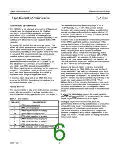
PINNING
SYMBOL
INH
PIN
DESCRIPTION
1
2
3
4
inhibit output for switching an external voltage regulator if a wake-up signal occurs
transmit data input for activating the driver to the bus lines
TXD
RXD
ERR
receive data output for reading out the data from the bus lines
error, wake-up and power-on indication output; active LOW in normal operating mode when the
bus has a failure and in low power modes (wake-up signal or in power-on standby)
STB
EN
5
6
standby digital control signal input (active LOW); defines together with input signal on pin EN the
state of the transceiver (in normal and low power modes); see Table 2 and Fig.3
enable digital control signal input; defines together with input signal on pin STB the state of the
transceiver (in normal and low power modes); see Table 2 and Fig.3
WAKE
RTH
7
8
local wake-up signal input; falling and rising edges are both detected
termination resistor connection; in case of a CANH bus wire error the line is terminated with a
selectable impedance
RTL
9
termination resistor connection; in case of a CANL bus wire the line is terminated with a
selectable impedance
VCC
10 supply voltage
CANH
CANL
GND
BAT
11 HIGH-level voltage bus line
12 LOW-level voltage bus line
13 ground
14 battery supply
handbook, halfpage
INH
1
2
3
4
5
6
7
14 BAT
13
TXD
RXD
GND
12 CANL
11
TJA1054T
ERR
STB
CANH
10
9
V
CC
EN
RTL
RTH
WAKE
8
MGL422
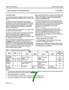
Fig.2 Pin configuration.
5
1999 Feb 11

 NXP [ NXP ]