Philips Semiconductors
Preliminary specification
VIF-PLL demodulator and FM-PLL detector
TDA9800
SYMBOL
PARAMETER
CONDITIONS
MIN.
TYP.
MAX.
UNIT
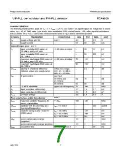
Vi IF
IF input signal sensitivity
(RMS value, pins 1 and 2)
for PLL still locked
maximum IF gain;
note 5
−
50
90
µV
for C/N = 10 dB
note 6
−
−
100
140
µV
µA
Iloop
FPLL loop offset current at pin 6
note 7
−
±4.5
sound carrier off
Composite video amplifier (pin 13)
V0 vid
V13
output signal (peak-to-peak value)
see Fig.7
0.9
1.4
−
1.0
1.5
2.6
1.1
1.6
−
V
sync level
V
zero carrier level
V
upper video clipping level
lower video clipping level
IF intercarrier level (RMS value)
output resistance
VP − 1.1 VP − 1.0
−
V
−
0.3
170
−
0.4
−
V
V0 FM
R13
sound carrier on; note 8 −
mV
Ω
−
10
−
Iint13
internal bias current for emitter
follower
DC
1.8
2.5
mA
I13
maximum output sink current
maximum output source current
−3 dB video bandwidth
DC and AC
1.4
2.0
7
−
−
−
−
−
mA
mA
MHz
dB
−
B
C13 < 50 pF; RL >1 kΩ
10
40
αH
suppression of video signal
harmonics
C13 < 50 pF; RL >1 kΩ; 35
note 9
RR
ripple rejection on pin 13
see Fig.9
32
35
−
dB
CVBS buffer amplifier and noise clipper (pins 7 and 14)
R14
input resistance
input capacitance
DC voltage at input
voltage gain
2.6
1.4
1.5
6
3.3
2
4.0
3.0
2.1
7.5
2.3
kΩ
pF
V
C14
V14
pin 14 not connected
note 10
1.8
7
Gv
dB
V
Vo CVBS
CVBS output signal on pin 7
(peak-to-peak value)
sound carrier off;
see Fig.3
1.7
2.0
CVBS output level
output resistance
upper video clipping
lower video clipping
sync level
3.9
−
4.0
1.0
1.35
−
−
V
1.1
−
V
−
V
R7
−
10
−
Ω
Iint7
internal bias current for emitter
follower
DC
1.8
2.5
mA
I7
B
maximum output sink current
maximum output source current
−3 dB video bandwidth
DC and AC
1.4
2.4
8
−
−
−
−
mA
−
mA
C7 < 20 pF; RL > 1 kΩ
11
MHz
July 1994
8

 NXP [ NXP ]