Philips Semiconductors
Preliminary specification
VIF-PLL demodulator and FM-PLL detector
TDA9800
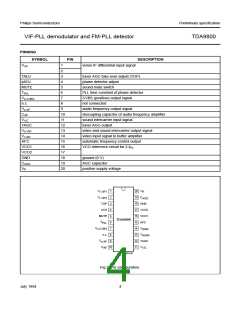
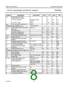
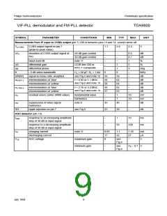
PINNING
SYMBOL
PIN
DESCRIPTION
Vi IF
1
vision IF differential input signal
2
TADJ
3
tuner AGC take-over adjust (TOP)
phase detector adjust
φADJ
4
MUTE
TPLL
5
sound mute switch
6
PLL time constant of phase detector
CVBS (positive) output signal
not connected
Vo CVBS
n.c.
7
8
Vo AF
CAF
9
audio frequency output signal
decoupling capacitor of audio frequency amplifier
sound intercarrier input signal
tuner AGC output
10
11
12
13
14
15
16
17
18
19
20
Vi IC
TAGC
Vo VID
Vi VID
AFC
video and sound intercarrier output signal
video input signal to buffer amplifier
automatic frequency control output
VCO reference circuit for 2 fPC
VCO1
VCO2
GND
CAGC
VP
ground (0 V)
AGC capacitor
positive supply voltage
handbook, halfpage
V
V
V
P
1
2
20
19
i VIF1
C
i VIF2
TOP
AGC
3
18 GND
17
CCS
VCO2
4
MUTE
16 VCO1
15 AFC
5
TDA9800
T
6
PLL
V
V
V
7
14
13
12
11
o CVBS
n.c.
i(vid)
8
o(vid)
V
TAGC
9
o AF
V
C
10
i IC
AF
MED330
Fig.2 Pin configuration.
July 1994
4

 NXP [ NXP ]