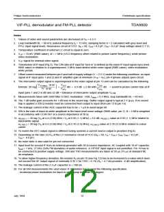
Philips Semiconductors
Preliminary specification
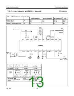
VIF-PLL demodulator and FM-PLL detector
TDA9800
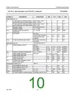
SYMBOL
PARAMETER
CONDITIONS
MIN.
TYP.
MAX.
UNIT
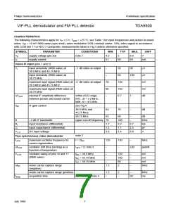
Measurements from IF input to CVBS output (pin 7) 330 Ω between pins 13 and 14, sound carrier off
Vo CVBS
CVBS output signal on pin 7
(peak-to-peak value)
1.7
2.0
2.3
V
∆Vo
deviation of CVBS output signal at
B/G
50 dB gain control
30 dB gain control
note 11
−
−
0.5
0.1
1
dB
dB
%
−
−
black level tilt
−
−
∆G
differential gain
CCIR line 330 or
NTC-7 Composite
−
2
5
%
∆ϕ
differential phase
−
1
3
deg
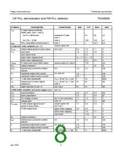
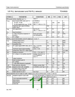
MHz
dB
dB
dB
dB
dB
mV
mV
dB
B
−3 dB video bandwidth
signal-to-noise ratio; weighted
intermodulation at ‘blue’
intermodulation at ‘yellow’
intermodulation at ‘blue’
intermodulation at ‘yellow’
residual vision carrier (RMS value)
CL < 20 pF; RL > 1 kΩ
6
8
−
S/N(W)
α0.92/1.1
see Fig.5 and note 12
56
56
58
56
57
−
59
62
64
62
63
1
−
f = 0.92 or 1.1 MHz;
see Fig.6 and note 13
−
−
α2.76/3.3
f = 2.76 or 3.3 MHz;
see Fig.6 and note 13
−
−
αC
fundamental wave
harmonics
10
10
−
−
1
αH
suppression of video signal
harmonics
note 9
35
40
RR
ripple rejection on pin 7
see Fig.9
25
28
−
dB
AGC detector (pin 19)
tresp
response to an increasing amplitude
step of 50 dB in input signal
−
−
1
10
ms
ms
response to a decreasing amplitude
step of 50 dB in input signal
50
100
I19
charging current
discharging current
AGC voltage
note 11
0.85
17
0
1.1
22
1.35
27
−
mA
µA
V
V19
maximum gain
minimum gain
see
Fig.4
−
see
VP − 0.7 V
Fig.4
July 1994
9

 NXP [ NXP ]