TDA8931
Philips Semiconductors
Power comparator 1 × 20 W
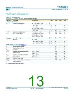
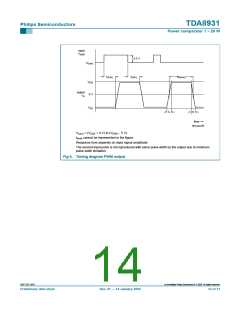
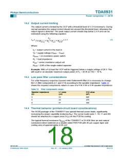
input
V
i(dif)
3.3 V
V
i(cm)
t
t
t
W(min)
r(LH)
r(HL)
V
DD
output
0 V
V
o
V
SS
t
t
f
r
time
001aac235
Vi(cm) = (VSSA + 4 V) to (VDDA − 5 V).
tdead cannot be represented in the figure.
Response time depends on input signal amplitude.
The second input pulse is not reproduced with same pulse width by the output due to minimum
pulse width limitation.
Fig 4. Timing diagram PWM output
9397 750 13847
© Koninklijke Philips Electronics N.V. 2005. All rights reserved.
Preliminary data sheet
Rev. 01 — 14 January 2004
14 of 31

 NXP [ NXP ]