TDA8931
Philips Semiconductors
Power comparator 1 × 20 W
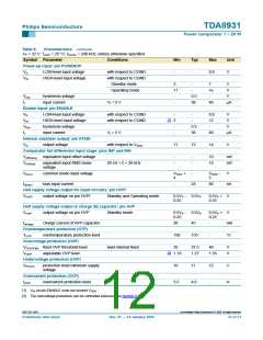
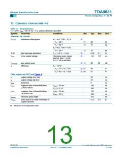
13. Dynamic characteristics
Table 10: Characteristics
VP = 22 V; Tamb = 25 °C; RL = 4 Ω; unless otherwise specified.
Symbol
Parameter
Conditions
Min
Typ
Max
Unit
Amplifier; SE channel
[1]
Po(max)
maximum output power
RL = 4 Ω; THD = 10 %
VP = 26 V
21
15
22
16
-
-
W
W
VP = 22 V
RL = 8 Ω; THD =10 %
VP = 30 V
15
-
16
-
W
%
[1]
[1]
THD
Vn(o)
total harmonic distortion
noise output voltage
Po = 1 W, fi = 1 kHz
0.02
128
0.1
150
Operating mode; inputs
shorted; gain = 20 dB,
AES17 brick wall filter
-
µV
[1]
Gv(range)
gain adjust range
efficiency
14
20
26
dB
η
Po = 15 W
[1]
[1]
Vp = 22 V; RL = 4 Ω
Vp = 30 V; RL = 8 Ω
87
89
89
91
-
-
%
%
PWM output: pin OUT (see Figure 4)
tr
output voltage rise time
output voltage fall time
dead time
-
-
-
-
-
-
-
-
-
20
-
ns
ns
ns
ns
ns
ns
ns
ns
Ω
tf
20
-
tdead
tr(LH)
0
-
response time of transition from
LOW-to-HIGH
Vi(dif) = 70 mV
Vi(dif) = 3.3 V
Vi(dif) = 70 mV
Vi(dif) = 3.3 V
120
100
120
100
150
0.22
-
-
tr(HL)
response time of transition from
HIGH-to-LOW
-
-
tW(min)
RDSon
minimum pulse width
-
drain-source on-state resistance of
output transistor
0.3
[1] Measured in the application board.
9397 750 13847
© Koninklijke Philips Electronics N.V. 2005. All rights reserved.
Preliminary data sheet
Rev. 01 — 14 January 2004
13 of 31

 NXP [ NXP ]