Philips Semiconductors
Product specification
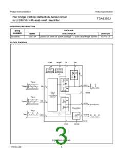
Full bridge vertical deflection output circuit
in LVDMOS with east-west amplifier
TDA8358J
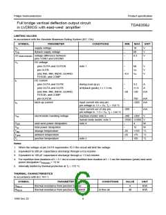
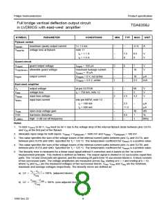
LIMITING VALUES
In accordance with the Absolute Maximum Rating System (IEC 134).
SYMBOL
PARAMETER
supply voltage
flyback supply voltage
CONDITIONS
MIN. MAX. UNIT
VP
VFB
−
−
−
18
68
0.3
V
V
V
∆VVGND-EWGND voltage difference between
pins VGND and EWGND
Vn
DC voltage
pins OUTA and OUTEW
pin OUTB
note 1
−
68
VP
VP
V
V
V
−
pins INA, INB, INEW, GUARD,
FEEDB, and COMP
−0.5
In
DC current
pins OUTA and OUTB
pins OUTA and OUTB
during scan (p-p)
−
3.2
A
at flyback (peak); t ≤ 1.5 ms
−
±1.8
+20
A
pins INA, INB, INEW, GUARD,
FEEDB, and COMP
−20
mA
pin OUTEW
−
−
750
mA
Ilu
latch-up current
input current into any pin;
+200 mA
pin voltage is 1.5 × VP; Tj = 150 °C
input current out of any pin;
pin voltage is −1.5 × VP; Tj = 150 °C
−200
−300
−
mA
Ves
electrostatic handling voltage
machine model; note 2
human body model; note 3
note 4
+300
V
−2000 +2000 V
PEW
Ptot
Tstg
Tamb
Tj
east-west power dissipation
total power dissipation
storage temperature
−
4
W
W
−
15
−55
−25
−
+150 °C
ambient temperature
junction temperature
+75
150
°C
°C
note 5
Notes
1. When the voltage at pin OUTA supersedes 70 V the circuit will limit the voltage.
2. Equivalent to 200 pF capacitance discharge through a 0 Ω resistor.
3. Equivalent to 100 pF capacitance discharge through a 1.5 kΩ resistor.
4. For repetitive time durations of t < 0.1 ms or a non repetitive time duration of t < 5 ms the maximum (peak) east-west
power dissipation PEW(peak) = 15 W.
5. Internally limited by thermal protection at Tj ≈ 170 °C.
THERMAL CHARACTERISTICS
In accordance with IEC 747-1.
SYMBOL
Rth(j-c)
PARAMETER
CONDITIONS
VALUE
UNIT
K/W
K/W
thermal resistance from junction to case
thermal resistance from junction to ambient
4
Rth(j-a)
in free air
40
1999 Dec 22
6

 NXP [ NXP ]