Philips Semiconductors
Product specification
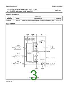
Full bridge vertical deflection output circuit
in LVDMOS with east-west amplifier
TDA8358J
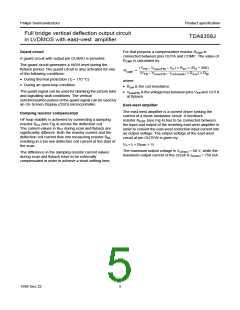
PINNING
SYMBOL
FUNCTIONAL DESCRIPTION
Vertical output stage
PIN
DESCRIPTION
The vertical driver circuit has a bridge configuration.
The deflection coil is connected between the
INA
1
2
input A
input B
INB
complimentary driven output amplifiers. The differential
input circuit is voltage driven. The input circuit is specially
designed for direct connection to driver circuits delivering
a differential signal but it is also suitable for single-ended
applications. The output currents of the driver device are
converted to voltages by the conversion resistors
VP
3
supply voltage
output B
OUTB
INEW
VGND
EWGND
OUTEW
VFB
4
5
east-west input
vertical ground
east-west ground
east-west output
flyback supply voltage
output A
6
7
RCV1 and RCV2 (see Fig.3) connected to pins INA
8
and INB. The differential input voltage is compared with
the voltage across the measuring resistor RM, providing
internal feedback information. The voltage across RM is
proportional with the output current. The relationship
between the differential input current and the output
current is defined by:
9
OUTA
GUARD
FEEDB
COMP
10
11
12
13
guard output
feedback input
compensation input
2 × Ii(dif)(p-p) × RCV = Io(p-p) × RM
The output current should measure 0.5 to 3.2 A (p-p) and
is determined by the value of RM and RCV. The allowable
input voltage range is 100 mV to 1.6 V for each input. The
formula given does not include internal bondwire
resistances. Depending on the value of RM and the internal
bondwire resistance (typical value 50 mΩ) the actual value
of the current in the deflection coil will be about 5% lower
than calculated.
handbook, halfpage
INA
INB
1
2
3
4
5
6
7
8
9
V
P
OUTB
Flyback supply
INEW
VGND
The flyback voltage is determined by the flyback supply
voltage VFB. The principle of two supply voltages (class G)
allows to use an optimum supply voltage VP for scan and
an optimum flyback supply voltage VFB for flyback, thus
very high efficiency is achieved. The available flyback
output voltage across the coil is almost equal to VFB, due
to the absence of a coupling capacitor which is not
required in a bridge configuration. The very short
TDA8358J
EWGND
OUTEW
V
FB
OUTA 10
GUARD 11
FEEDB 12
COMP 13
rise and fall times of the flyback switch are determined
mainly by the slew-rate value of more than 300 V/µs.
Protection
MGL867
The output circuit contains protection circuits for:
•
•
Too high die temperature
Overvoltage of output A.
The die has been glued to the metal block of the package. If the metal
block is not insulated from the heatsink, the heatsink shall only be
connected directly to pin VGND.
Fig.2 Pin configuration.
1999 Dec 22
4

 NXP [ NXP ]