Philips Semiconductors
Product specification
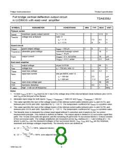
Full bridge vertical deflection output circuit
in LVDMOS with east-west amplifier
TDA8358J
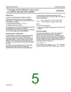
Guard circuit
For that purpose a compensation resistor RCMP is
connected between pins OUTA and COMP. The value of
RCMP is calculated by:
A guard circuit with output pin GUARD is provided.
The guard circuit generates a HIGH-level during the
flyback period. The guard circuit is also activated for one
of the following conditions:
(VFB – Vloss(FB) – VP) × RD1 × (RS + 300)
RCMP
=
-------------------------------------------------------------------------------------------------------------
(VFB – Vloss(FB) – Icoil(peak) × Rcoil) × RM
• During thermal protection (Tj ≈ 170 °C)
• During an open-loop condition.
where:
• Rcoil is the coil resistance
The guard signal can be used for blanking the picture tube
and signalling fault conditions. The vertical
• Vloss(FB) is the voltage loss between pins VFB and OUTA
at flyback.
synchronization pulses of the guard signal can be used by
an On Screen Display (OSD) microcontroller.
East-west amplifier
The east-west amplifier is a current driver sinking the
current of a diode modulator circuit. A feedback
resistor REWF (see Fig.4) has to be connected between
the input and output of the inverting east-west amplifier in
order to convert the east-west correction input current into
an output voltage. The output voltage of the east-west
circuit at pin OUTEW is given by:
Damping resistor compensation
HF loop stability is achieved by connecting a damping
resistor RD1 (see Fig.4) across the deflection coil.
The current values in RD1 during scan and flyback are
significantly different. Both the resistor current and the
deflection coil current flow into measuring resistor RM,
resulting in a too low deflection coil current at the start of
the scan.
Vo ≈ Ii × REWF + Vi
The maximum output voltage is Vo(max) = 68 V, while the
maximum output current of the circuit is Io(max) = 750 mA.
The difference in the damping resistor current values
during scan and flyback have to be externally
compensated in order to achieve a short settling time.
1999 Dec 22
5

 NXP [ NXP ]