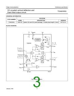
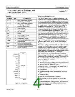
Philips Semiconductors
Preliminary specification
DC-coupled vertical deflection and
East-West output circuit
TDA8350Q
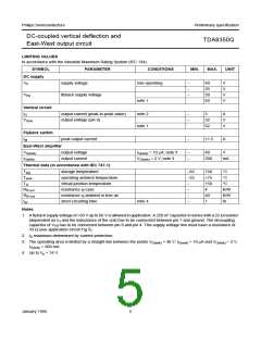
CHARACTERISTICS
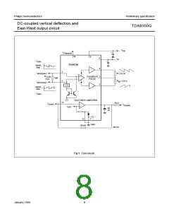
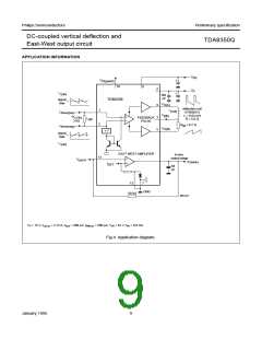
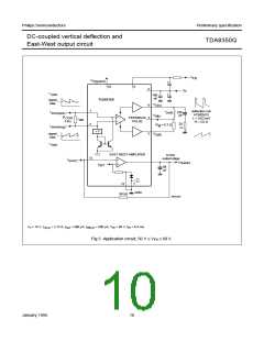
VP = 17.5 V; VFB = 45 V; VO(sink) = 20 V; fi = 50 Hz; II(sb) = 400 µA; Tamb = 25°C; measured in test circuit of Fig.3; unless
otherwise specified.
SYMBOL
PARAMETER
CONDITIONS
MIN.
TYP.
MAX.
UNIT
DC supply
VP
operating supply voltage
flyback supply voltage
9
−
25
V
VFB
Vp
−
−
50
60
55
V
note 1
−
V
IP
supply current
no signal; no load
−
30
mA
Vertical circuit
VO
LE
output voltage swing (scan)
Idiff = 0.6 mA (p-p);
19.8
−
−
V
V
diff = 1.8 V (p-p);
IO = 3 A (p-p)
linearity error
IO = 3 A (p-p);
−
−
−
1
2
2
−
%
%
V
IO = 50 mA (p-p); note 2
1
VO
output voltage swing (flyback)
VO(A) - VO(B)
Idiff = 0.3 mA;
IO = 1.5 A (M)
39
VDF
|Ios|
forward voltage of the internal
IO = −1.5 A (M);
Idiff = 0.3 mA
−
−
−
−
−
−
−
−
1.5
30
18
72
V
efficiency diode (VO(A) - VFB
)
output offset current
Idiff = 0;
mA
mV
µV/K
I
I(sb) = 50 to 500 µA
|Vos|
∆VosT
offset voltage at the input of the
feedback amplifier VI(fb) - VO(B)
Idiff = 0;
II(sb) = 50 to 500 µA
output offset voltage as a function Idiff = 0;
of temperature
VO(A)
Gv
DC output voltage
Idiff = 0; note 3
−
−
−
8
−
−
−
V
open loop voltage gain (V9-5/V1-2
)
notes 4 and 5
note 4
80
80
dB
dB
open loop voltage gain (V9-5/V3-5
V1-2 = 0)
;
VR
voltage ratio V1-2/V3-5
−
−
−
−
0
−
dB
Hz
fres
GI
frequency response (−3 dB)
note 6
40
−
current gain (IO/Idiff
)
5000
−
10−4
∆GIT
current gain drift as a function of
temperature
−
/K
II(sb)
signal bias current
50
−
400
−
500
100
−
µA
µA
dB
V
IFB
flyback supply current
power supply ripple rejection
DC voltage at the input
common mode input voltage
input bias current
during scan
note 7
PSRR
VI(DC)
VI(CM)
Ibias
−
80
2.7
−
−
−
II(sb) = 0
II(sb) = 0
0
1.6
0.5
−
V
−
0.1
0.2
µA
mA
IO(CM)
common mode output current
∆II(sb) = 300 µA (p-p);
−
fi = 50 Hz; Idiff = 0
January 1995
6

 NXP [ NXP ]