Philips Semiconductors
Preliminary specification
DC-coupled vertical deflection and
East-West output circuit
TDA8350Q
PINNING
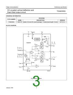
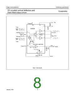
FUNCTIONAL DESCRIPTION
The vertical driver circuit is a bridge configuration. The
deflection coil is connected between the output amplifiers,
which are driven in phase opposition. An external resistor
(RM) connected in series with the deflection coil provides
internal feed back information. The differential input circuit
is voltage driven. The input circuit has been adapted to
enable it to be used with the TDA9150, TDA9151B,
TDA9160A, TDA9162, TDA8366 and TDA8367 which
deliver symmetrical current signals. An external resistor
(RCON) connected between the differential input
determines the output current through the deflection coil.
The relationship between the differential input current and
the output current is defined by: Idiff × RCON = I(coil) × RM.
The output current is adjustable from 0.5 A (p-p) to 3 A
(p-p) by varying RM. The maximum input differential
voltage is 1.8 V. In the application it is recommended that
SYMBOL
PIN
DESCRIPTION
Idrive(pos)
1
input power-stage (positive);
includes II(sb) signal bias
Idrive(neg)
2
input power-stage (negative);
includes II(sb) signal bias
VI(fb)
3
4
5
6
7
8
9
feedback voltage input
supply voltage
VP
VO(B)
n.c.
output voltage B
not connected
GND
VFB
ground
flyback supply voltage
output voltage A
VO(A)
VO(guard)
VO(sink)
10 guard output voltage
V
diff = 1.5 V (typ). This is recommended because of the
spread of input current and the spread in the value of
RCON
11
East-West amplifier driver (sink)
output voltage
.
II(corr)
II(set)
12 East-West amplifier input
correction current (negative)
The flyback voltage is determined by an additional supply
voltage VFB. The principle of operating with two supply
voltages (class G) makes it possible to fix the supply
voltage VP optimum for the scan voltage and the second
supply voltage VFB optimum for the flyback voltage. Using
this method, very high efficiency is achieved.
13 East-West amplifier set input
current (positive)
dbook, halfpage
The supply voltage VFB is almost totally available as
flyback voltage across the coil, this being possible due to
the absence of a decoupling capacitor (not necessary, due
to the bridge configuration). The output circuit is fully
protected against the following:
I
I
1
2
drive(pos)
drive(neg)
V
3
I(fb)
V
P
4
•
•
•
thermal protection
V
5
O(B)
short-circuit protection of the output pins (pins 5 and 9)
short-circuit of the output pins to VP.
n.c.
6
7
GND
TDA8350
A guard circuit VO(guard) is provided. The guard circuit is
activated at the following conditions:
V
8
FB
V
• during flyback
O(A)
9
• during various short-circuit possibilities at the output
pins
V
10
11
12
13
O(guard)
V
O(sink)
• during open loop
I
I(corr)
• when the thermal protection is activated.
I
I(set)
This signal can be used for blanking the picture tube
screen.
MBC226-1
An East-West amplifier is also provided. This amplifier is
an inverting amplifier which is current driven with sink
current only capabilities.
Fig.2 Pin configuration.
January 1995
4

 NXP [ NXP ]