Philips Semiconductors
Preliminary specification
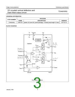
DC-coupled vertical deflection and
East-West output circuit
TDA8350Q
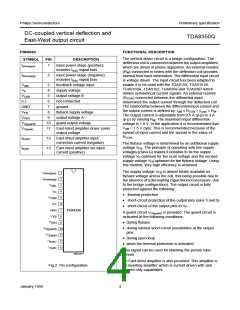
FEATURES
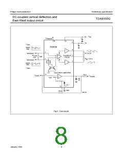
GENERAL DESCRIPTION
• Few external components
The TDA8350Q is a power circuit for use in 90° and 110°
colour deflection systems for field frequencies of 50
to 120 Hz. The circuit provides a DC driven vertical
deflection output circuit, operating as a highly efficient
class G system and an East-West driver for sinking the
diode modulator current.
• Highly efficient fully DC-coupled vertical output bridge
circuit
• Vertical flyback switch
• Guard circuit
• Protection against:
– short-circuit of the output pins
– short-circuit of the output pins to VP
• High EMC immunity due to common mode inputs
• Temperature (thermal) protection
• East-West output stage with one single conversion
resistor.
QUICK REFERENCE DATA
SYMBOL
PARAMETER
CONDITIONS
MIN.
TYP.
MAX.
UNIT
DC supply
VP
IP
supply voltage
9
−
25
V
quiescent current
−
30
−
mA
Vertical circuit
IO(p-p)
output current (peak-to-peak value)
−
−
−
3
A
Idiff(p-p)
differential input current
(peak-to-peak value)
600
−
µA
Vdiff(p-p)
differential input voltage
(peak-to-peak value)
−
1.5
1.8
V
Flyback switch
IM
peak output current
−
−
−
−
−
−
±1.5
50
A
V
V
VFB
flyback supply voltage
note 1
60
East-West amplifier
IO(sink)
VO(sink)
Ibias
output current (sink only)
−
−
−
−
−
−
500
40
1
mA
V
peak output voltage
input bias current
IO(sink) = 10 µA
µA
Thermal data (in accordance with IEC 747-1)
Tstg
Tamb
Tvj
storage temperature
−65
−25
−
−
−
−
150
+75
150
°C
°C
°C
operating ambient temperature
virtual junction temperature
Note
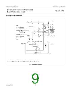
1. A flyback supply voltage of >50 V up to 60 V is allowed in application. A 220 nF capacitor in series with a 22 Ω resistor
(dependent on IO and the inductance of the coil) has to be connected between pin 7 and ground. The decoupling
capacitor of VFB has to be connected between pin 8 and pin 4. This supply voltage line must have a resistance of
33 Ω (see application circuit Fig.5).
January 1995
2

 NXP [ NXP ]