Philips Semiconductors
Preliminary specification
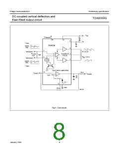
DC-coupled vertical deflection and
East-West output circuit
TDA8350Q
LIMITING VALUES
In accordance with the Absolute Maximum Rating System (IEC 134).
SYMBOL
DC supply
PARAMETER
CONDITIONS
MIN.
MAX.
UNIT
VP
supply voltage
non-operating
−
−
−
40
V
25
50
60
V
V
V
VFB
flyback supply voltage
note 1
Vertical circuit
IO
output current (peak-to-peak value)
output voltage (pin 9)
note 2
note 1
−
−
3
A
V
V
VO(A)
52
62
Flyback switch
IM
peak output current
−
±1.5
A
East-West amplifier
VO(sink)
output voltage
output current
IO(sink) = 10 µA; note 3
−
−
40
V
IO(sink)
VO(sink) = 2 V; note 3
500
mA
Thermal data (in accordance with IEC 747-1)
Tstg
storage temperature
−65
−25
−
150
+75
150
4
°C
Tamb
Tvj
operating ambient temperature
virtual junction temperature
resistance vj-case
°C
°C
Rth vj-c
Rth vj-a
tsc
−
K/W
K/W
hr
resistance vj-ambient in free air
short-circuiting time
−
40
1
note 4
−
Notes
1. A flyback supply voltage of >50 V up to 60 V is allowed in application. A 220 nF capacitor in series with a 22 Ω resistor
(dependent on IO and the inductance of the coil) has to be connected between pin 7 and ground. The decoupling
capacitor of VFB has to be connected between pin 8 and pin 4. This supply voltage line must have a resistance of
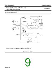
33 Ω (see application circuit Fig.5).
2. IO maximum determined by current protection.
3. The operating area is limited by a straight line between the points VO(sink) = 40 V; IO(sink) = 10 µA and VO(sink) = 2 V;
IO(sink) = 500 mA.
4. Up to Vp = 18 V.
January 1995
5

 NXP [ NXP ]