Philips Semiconductors
Preliminary specification
DC-coupled vertical deflection and
East-West output circuit
TDA8350Q
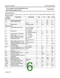
SYMBOL
PARAMETER
CONDITIONS
MIN.
TYP.
MAX.
UNIT
East-West amplifier
VO(sink)
saturation voltage
IO(sink) = 500 mA;
−
2.0
2.5
V
II(corr) = 0 µA; note 8
Gv
fres
LE
open loop voltage gain (V11/V12)
frequency response (−3 dB)
linearity error
−
−
−
−
−
−
−
−
47
−
dB
Hz
%
4000
−
VO(sink) = 3 V
−
−
−
1
1
−
1
VO(sink) = 10 V; note 2
0.5
2
%
Ibias
input bias current (pin 12)
DC input voltage
µA
V
VI(DC)
Iset
−
offset voltage set current
−
mA
V
V13-7
maximum allowed voltage at
pin 13
0.3
Guard circuit
IO
output current
not active;
−
−
50
µA
VO(guard) = 0 V
output current
active; VO(guard) = 4.5 V
1
−
−
−
−
−
2.5
5.5
40
mA
V
VO(guard)
output voltage
IO = 100 µA
allowable voltage on pin 10
maximum leakage
V
current = 10 µA
Notes
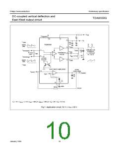
1. A flyback supply voltage of >50 V up to 60 V is allowed in application. A 220 nF capacitor in series with a 22 Ω resistor
(dependent on IO and the inductance of the coil) has to be connected between pin 7 and ground. The decoupling
capacitor of VFB has to be connected between pin 8 and pin 4. This supply voltage line must have a resistance of
33 Ω (see application circuit Fig.5).
2. The linearity error is measured without S-correction and based on the same measurement principle as performed on
the screen. The measuring method is as follows:
Divide the output signal I5 - I9 (VRM) into 22 equal parts ranging from 1 to 22 inclusive. Measure the value of two
succeeding parts called one block starting with part 2 and 3 (block 1) and ending with part 20 and 21 (block 10). Thus
part 1 and 22 are unused. The equations for linearity error for adjacent blocks (LEAB) and not adjacent blocks (NAB)
are given below;
ak – a(k + 1)
amax – amin
-----------------------------
aavg
LEAB =
; NAB =
-----------------------------
aavg
3. Referenced to VP.
4. V values within formulae, relate to voltages at or between relative pin numbers, i.e. V9-5/V1-2 = voltage value across
pins 9 and 5 divided by voltage value across pins 1 and 2.
5. V3-5 AC short-circuited.
6. Frequency response V9-5/V3-5 is equal to frequency response V9-5/V1-2
.
7. At V(ripple) = 500 mV eff; measured across RM; fi = 50 Hz.
8. The output pin 11 requires a capacitor of minimum value 68 nF.
January 1995
7

 NXP [ NXP ]