Philips Semiconductors
Product specification
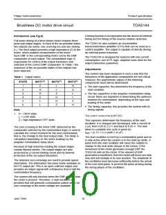
Brushless DC motor drive circuit
TDA5144
CHARACTERISTICS
VP = 14.5 V; Tamb = 25 °C; unless otherwise specified.
SYMBOL
Supply
PARAMETER
CONDITIONS
MIN.
TYP.
MAX.
UNIT
VP
supply voltage
note 1
note 2
4
−
18
V
IP
supply current
−
6.3
7.2
16
mA
V
VVMOT
input voltage to the output driver
stages
see Fig.1
1.7
−
Thermal protection
TSD
local temperature at temperature
130
140
150
°C
sensor causing shut-down
∆T
reduction in temperature before
switch-on
after shut-down
−
TSD − 30 −
K
MOT0; centre tap
VI
input voltage
−0.5
−
VVMOT
0
V
II
input bias current
0.5 V < VI < VVMOT − 1.5 V −10
−
µA
mV
mV
VCSW
∆VCSW
comparator switching level
note 3
±20
−3
±25
0
±30
+3
variation in comparator switching
levels
Vhys
comparator input hysteresis
−
75
−
µV
MOT1, MOT2 and MOT3
VDO
drop-out output voltage
IO = 100 mA
IO = 1000 mA
IO = 100 mA
−
−
−
0.9
1.6
−
1.05
1.85
180
V
V
∆VOL
∆VOH
variation in saturation voltage
between lower transistors
mV
variation in saturation voltage
between upper transistors
IO = −100 mA
−
−
180
mV
ILIM
tr
current limiting
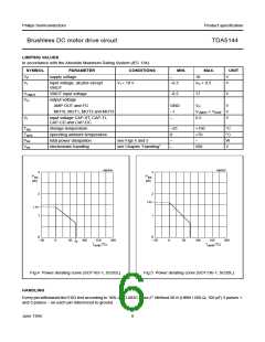
VVMOT = 10 V; RO = 1.2 Ω 1.8
2.0
10
15
−
2.5
15
A
rise time switching output
fall time switching output
diode forward voltage (diode DH)
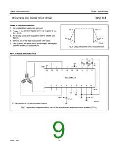
VVMOT = 15 V; see Fig.6
VVMOT = 15 V; see Fig.6
5
µs
µs
V
tf
10
−
20
VDHF
IO = −500 mA;
1.5
notes 4 and 5; see Fig.1
VDLF
IDM
diode forward voltage (diode DL)
IO = 500 mA;
notes 4 and 5; see Fig.1
−1.5
−
−
−
V
A
peak diode current
note 5
−
2.5
+AMP IN and −AMP IN
VI
input voltage
−0.3
−
−
VP − 1.7
±VP
V
V
differential mode voltage without
‘latch-up’
−
Ib
input bias current
input capacitance
input offset voltage
−
−
−
−
4
−
650
−
nA
pF
CI
Voffset
10
mV
June 1994
7

 NXP [ NXP ]