Philips Semiconductors
Product specification
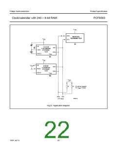
Clock/calendar with 240 × 8-bit RAM
PCF8583
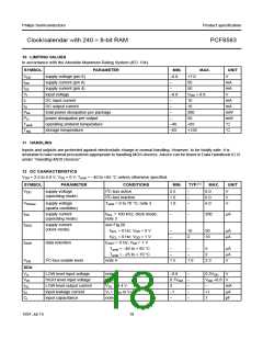
10 LIMITING VALUES
In accordance with the Absolute Maximum Rating System (IEC 134).
SYMBOL
PARAMETER
MIN.
−0.8
MAX.
UNIT
VDD
IDD
ISS
VI
supply voltage (pin 8)
supply current (pin 8)
supply current (pin 4)
input voltage
+7.0
50
V
−
mA
mA
V
−
50
−0.8
−
VDD + 0.8
10
II
DC input current
mA
mA
mW
mW
°C
IO
DC output current
−
10
Ptot
PO
Tamb
Tstg
total power dissipation per package
power dissipation per output
operating ambient temperature
storage temperature
−
300
50
−
−40
−65
+85
+150
°C
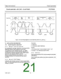
11 HANDLING
Inputs and outputs are protected against electrostatic charge in normal handling. However, to be totally safe, it is
desirable to take normal precautions appropriate to handling MOS devices. Advice can be found in Data Handbook IC12
under “Handling MOS Devices”.
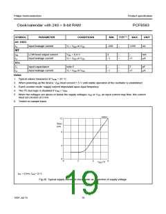
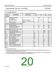
12 DC CHARACTERISTICS
V
DD = 2.5 to 6.0 V; VSS = 0 V; Tamb = −40 to +85 °C unless otherwise specified.
SYMBOL PARAMETER CONDITIONS
supply voltage
I2C-bus active
MIN.
2.5
TYP.(1)
MAX.
6.0
UNIT
VDD
−
V
(operating mode)
I2C-bus inactive
1.0
1.0
−
−
6.0
6.0
V
V
VDDosc
IDD
supply voltage
Tamb = 0 to 70 °C; note 2
(quartz oscillator)
supply current
(operating mode)
fSCL = 100 kHz; clock mode;
note 3
−
−
200
µA
IDDO
supply current
(clock mode)
see Fig.20
fSCL = 0 Hz; VDD = 5 V
SCL = 0 Hz; VDD = 1 V
−
−
10
2
50
10
µA
µA
f
IDDR
data retention
fOSCI = 0 Hz; VDD = 1 V
T
amb = −40 to + 85 °C
amb = −25 to + 70 °C
−
−
5
µA
µA
V
T
−
−
2
VEN
I2C-bus enable level
note 4
1.5
1.9
2.3
SDA
VIL
VIH
IOL
ILI
LOW level input voltage
HIGH level input voltage
LOW level output current
input leakage current
input capacitance
note 5
−0.8
−
−
−
−
−
0.3VDD
V
note 5
0.7VDD
VDD +0.8 V
VOL = 0.4 V
VI = VDD or VSS
note 6
3
−
mA
−1
−
+1
7
µA
Ci
pF
1997 Jul 15
18

 NXP [ NXP ]