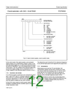
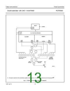
Philips Semiconductors
Product specification
Clock/calendar with 240 × 8-bit RAM
PCF8583
9
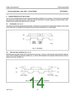
I2C-BUS PROTOCOL
Addressing
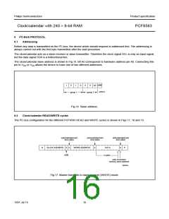
9.1
Before any data is transmitted on the I2C-bus, the device which should respond is addressed first. The addressing is
always carried out with the first byte transmitted after the start procedure.
The clock/calendar acts as a slave receiver or slave transmitter. Therefore the clock signal SCL is only an input signal,
but the data signal SDA is a bidirectional line.
The clock/calendar slave address is shown in Fig.16. Bit A0 corresponds to hardware address pin A0. Connecting this
pin to VDD or VSS allows the device to have one of two different addresses.
handbook, halfpage
1
0
1
0
0
0
A0 R/W
MRB016
group 2
group 1
Fig.16 Slave address.
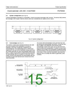
9.2
Clock/calendar READ/WRITE cycles
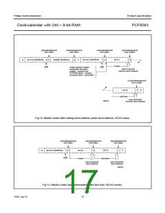
The I2C-bus configuration for the different PCF8583 READ and WRITE cycles is shown in Figs 17, 18 and 19.
acknowledgement
from slave
acknowledgement
from slave
acknowledgement
from slave
handbook, full pagewidth
S
SLAVE ADDRESS
0
A
WORD ADDRESS
A
DATA
A
P
R/W
n bytes
auto increment
memory word address
MBD822
Fig.17 Master transmits to slave receiver (WRITE) mode.
1997 Jul 15
16

 NXP [ NXP ]