Philips Semiconductors
Product specification
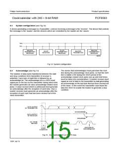
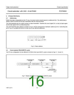
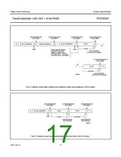
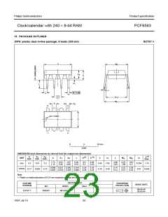
Clock/calendar with 240 × 8-bit RAM
PCF8583
SYMBOL
PARAMETER
CONDITIONS
MIN.
TYP.(1)
MAX.
UNIT
A0; OSCI
ILI
input leakage current
Vl = VDD or VSS
−250
−
+250
nA
INT
IOL
ILI
LOW level output current
input leakage current
VOL = 0.4 V
3
−
−
−
mA
Vl = VDD or VSS
−1
+1
µA
SCL
Ci
ILI
input capacitance
note 6
−
−
−
7
pF
input leakage current
VI = VDD or VSS
−1
+1
µA
Notes
1. Typical values measured at Tamb = 25 °C.
2. When powering-up the device, VDD must exceed 1.5 V until stable operation of the oscillator is established.
3. Event counter mode: supply current dependant upon input frequency.
4. The I2C-bus logic is disabled if VDD < VEN
.
5. When the voltages are above or below the supply voltages VDD or VSS, an input current may flow; this current
must not exceed ±0.5 mA.
6. Tested on sample basis.
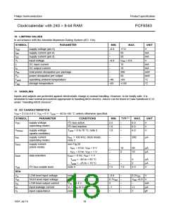
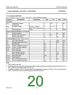
MRB012
12
handbook, halfpage
I
DDO
(µA)
8
4
0
0
2
4
6
V
(V)
DD
fSCL = 32 kHz; Tamb = 25 °C.
Fig.20 Typical supply current in clock mode as a function of supply voltage.
1997 Jul 15
19

 NXP [ NXP ]