PCA9675
NXP Semiconductors
Remote 16-bit I/O expander for Fm+ I2C-bus with interrupt
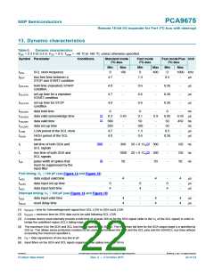
10.3 Differences between the PCA9675 and the PCF8575
The PCA9675 is a drop in replacement for the PCF8575 and can used without electrical
or software modifications, but there is a difference in interrupt output release timing during
the read operation.
Write operations are identical. At the completion of each 8-bit write sequence the data is
stored in its associated 8-bit write register at ACK or NACK. The first byte goes to P0n
while the second goes to P1n. Subsequent writes without a STOP wrap around to P0n
then P1n again. Any write will update both read registers and clear interrupts.
Read operations are identical. Both devices update the byte register with the pin data as
each 8-bit read is initiated, the very first read after an address cycle corresponds to ports
P0n while the second (even byte) corresponds to P1n and subsequent reads without a
STOP wrap around to P0n then P1n again.
During read operations, the PCA9675 interrupt output will be cleared in a byte-wise
fashion as each byte is read. Reading the first byte will clear any interrupts associated
with the P0n pins. This first byte read operation will have no effect on interrupts associated
with changes of state on the P1n pins. Interrupts associated with the P1n pins will be
cleared when the second byte is read. Reading the second byte has no effect on
interrupts associated with the changes of state on the P0x pins. The PCF8575 interrupt
output will clear after reading both bytes of data regardless of whether data was changed
in the first byte or the second byte or both bytes.
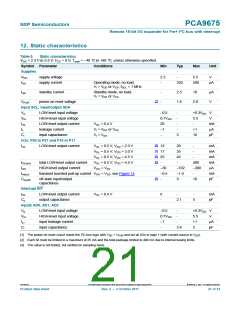
11. Limiting values
Table 4.
Limiting values
In accordance with the Absolute Maximum Rating System (IEC 60134).
Symbol
VDD
IDD
Parameter
Conditions
Min
Max
+6
Unit
V
supply voltage
0.5
supply current
-
100
600
5.5
mA
mA
V
ISS
ground supply current
input voltage
-
VI
VSS 0.5
II
input current
-
20
50
600
200
+150
+85
mA
mA
mW
mW
C
[1]
IO
output current
-
Ptot
P/out
Tstg
Tamb
total power dissipation
power dissipation per output
storage temperature
ambient temperature
-
-
65
40
operating
C
[1] Total package (maximum) output current is 600 mA.
PCA9675
All information provided in this document is subject to legal disclaimers.
© NXP B.V. 2011. All rights reserved.
Product data sheet
Rev. 2 — 3 October 2011
20 of 34

 NXP [ NXP ]