PCA9675
NXP Semiconductors
Remote 16-bit I/O expander for Fm+ I2C-bus with interrupt
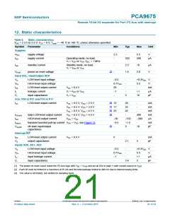
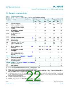
13. Dynamic characteristics
Table 6.
Dynamic characteristics
VDD = 2.3 V to 5.5 V; VSS = 0 V; Tamb = 40 C to +85 C; unless otherwise specified.
Symbol Parameter
Conditions
Standard mode
I2C-bus
Fast mode
I2C-bus
Fast modePlus Unit
I2C-bus
Min
0
Max
100
-
Min
0
Max
Min
0
Max
fSCL
SCL clock frequency
400
-
1000 kHz
tBUF
bus free time between a
STOP and START condition
4.7
1.3
0.5
-
-
-
-
-
s
s
s
s
ns
tHD;STA
tSU;STA
tSU;STO
hold time (repeated) START
condition
4.0
4.7
4.0
-
-
-
0.6
0.6
0.6
-
-
-
0.26
0.26
0.26
set-up time for a repeated
START condition
set-up time for STOP
condition
tHD;DAT
tVD;ACK
tVD;DAT
tSU;DAT
tLOW
data hold time
0
-
0
-
0
[1]
[2]
data valid acknowledge time
data valid time
0.3
300
250
4.7
4.0
3.45
0.1
50
0.9
0.05
50
0.45 s
-
-
-
-
-
-
-
-
450
ns
ns
s
s
data set-up time
100
1.3
0.6
50
-
-
-
LOW period of the SCL clock
0.5
0.26
tHIGH
HIGH period of the SCL
clock
[3][4]
[5]
[5]
tf
fall time of both SDA and
SCL signals
-
-
-
300
20 + 0.1Cb
300
300
50
-
-
-
120
120
50
ns
ns
ns
tr
rise time of both SDA and
SCL signals
1000 20 + 0.1Cb
[6]
tSP
pulse width of spikes that
must be suppressed by the
input filter
50
-
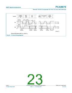
Port timing; CL 100 pF (see Figure 14 and Figure 15)
tv(Q)
tsu(D)
th(D)
data output valid time
data input set-up time
data input hold time
-
4
-
-
4
-
-
4
-
s
s
s
0
4
0
4
0
4
-
-
-
Interrupt timing; CL 100 pF (see Figure 14 and Figure 15)
tv(D)
data input valid time
reset delay time
-
-
4
4
-
-
4
4
-
-
4
4
s
s
td(rst)
[1] tVD;ACK = time for Acknowledgement signal from SCL LOW to SDA (out) LOW.
[2] tVD;DAT = minimum time for SDA data out to be valid following SCL LOW.
[3] A master device must internally provide a hold time of at least 300 ns for the SDA signal (refer to the VIL of the SCL signal) in order to
bridge the undefined region SCL’s falling edge.
[4] The maximum tf for the SDA and SCL bus lines is specified at 300 ns. The maximum fall time for the SDA output stage tf is specified at
250 ns. This allows series protection resistors to be connected between the SDA and the SCL pins and the SDA/SCL bus lines without
exceeding the maximum specified tf.
[5] Cb = total capacitance of one bus line in pF.
[6] Input filters on the SDA and SCL inputs suppress noise spikes less than 50 ns.
PCA9675
All information provided in this document is subject to legal disclaimers.
© NXP B.V. 2011. All rights reserved.
Product data sheet
Rev. 2 — 3 October 2011
22 of 34

 NXP [ NXP ]