PCA9675
NXP Semiconductors
Remote 16-bit I/O expander for Fm+ I2C-bus with interrupt
8. I/O programming
8.1 Quasi-bidirectional I/O architecture
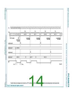
The PCA9675’s 16 ports (see Figure 2) are entirely independent and can be used either
as input or output ports. Input data is transferred from the ports to the microcontroller in
the Read mode (see Figure 15). Output data is transmitted to the ports in the Write mode
(see Figure 14).
Every data transmission from the PCA9675 must consist of an even number of bytes, the
first byte will be referred to as P07 to P00, and the second byte as P17 to P10. The third
will be referred to as P07 to P00, and so on.
This quasi-bidirectional I/O can be used as an input or output without the use of a control
signal for data directions. At power-on the I/Os are HIGH. In this mode only a current
source (IOH) to VDD is active. An additional strong pull-up to VDD (Itrt(pu)) allows fast rising
edges into heavily loaded outputs. These devices turn on when an output is written HIGH,
and are switched off by the negative edge of SCL. The I/Os should be HIGH before being
used as inputs. After power-on, as all the I/Os are set HIGH, all of them can be used as
inputs. Any change in setting of the I/Os as either inputs or outputs can be done with the
write mode.
Remark: If a HIGH is applied to an I/O which has been written earlier to LOW, a large
current (IOL) will flow to VSS
.
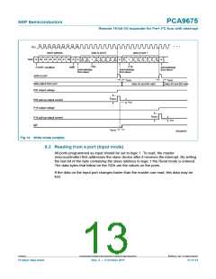
8.2 Writing to the port (Output mode)
To write, the master (microcontroller) first addresses the slave device. By setting the last
bit of the byte containing the slave address to logic 0 the Write mode is entered. The
PCA9675 acknowledges and the master sends the first data byte for P07 to P00. After the
first data byte is acknowledged by the PCA9675, the second data byte P17 to P10 is sent
by the master. Once again, the PCA9675 acknowledges the receipt of the data. Each 8-bit
data is presented on the port lines after it has been acknowledged by the PCA9675.
The number of data bytes that can be sent successively is not limited. After every two
bytes, the previous data is overwritten.
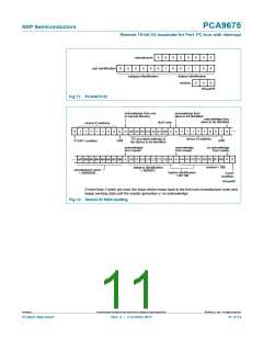
The first data byte in every pair refers to Port 0 (P07 to P00), whereas the second data
byte in every pair refers to Port 1 (P17 to P10) (see Figure 13).
first byte
second byte
07 06 05 04 03 02 01 00
P07 P06 P05 P04 P03 P02 P01 P00
A
17 16 15 14 13 12 11 10
P17 P16 P15 P14 P13 P12 P11 P10
A
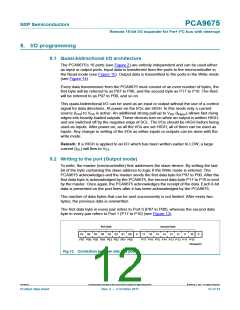
002aab634
Fig 13. Correlation between bits and ports
PCA9675
All information provided in this document is subject to legal disclaimers.
© NXP B.V. 2011. All rights reserved.
Product data sheet
Rev. 2 — 3 October 2011
12 of 34

 NXP [ NXP ]