Philips Semiconductors
Product specification
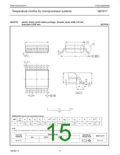
Temperature monitor for microprocessor systems
NE1617
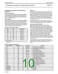
Configuration register
Conversion rate register
The configuration register is used to mask the Alert interrupt and/or
to put the device in software standby mode. Only two bits 6 and 7 of
this register are used as listed in Table 3. Bit 7 is used to mask the
device ALERT output from Alert interruption when this bit is set to 1
and bit 6 is used to activate the standby software mode when this bit
is set to to 1.
The conversion rate register is used to store programmable
conversion data, which defines the time interval between
conversions in standard free-running auto-convert mode. The
Table 5 shows all applicable data and rates for the device. Only
three LSB bits of the register are used and other bits are reserved
for future use. This register can be written to and read back over the
SMBus using commands of the registers named WCR and RCR
respectively. The POR default conversion data is 02h (0.25Hz).
This register can be written or read using the commands of registers
named WC and RC accordingly. Upon power-on reset (POR), both
bits are reset to zero.
Notice that the average supply current, as well as the device power
consumption, is increased with the conversion rate.
Table 3. Configuration register bit assignments
Table 5. Conversion rate control byte
POR
STATE
BIT
NAME
FUNCTION
DATA
CONVERSION
RATE (Hz)
AVERAGE
SUPPLY CURRENT
7 (MSB)
MASK
0
Mask ALERT interrupt:
Interrupt is enabled when
this bit is LOW, and disabled
when this bit is HIGH.
(µA Typ. @ V = 3.3V)
DD
00h
01h
0.0625
TBD
TBD
TBD
TBD
TBD
TBD
TBD
TBD
n/a
0.125
6
RUN/STOP
RESERVED
0
Standby or run mode
control:
When LOW, running mode is
enabled. When HIGH,
standby mode is initiated.
02h
0.25
03h
0.5
04h
1
05h
2
5 to 0
n/a
n/a
06h
4
8
07h
External and internal temperature registers
Results of temperature measurements after every ADC conversion
are stored in two registers: Internal Temp register (RIT) for internal
or local diode temperature, and External Temp register (RET) for
external or remote diode temperature. These registers can be only
read over the SMBus. The reading temperature data is in 2’s
complement binary form consisting of 7-bit data and 1-bit sign
(MSB), with each data count represents 1°C, and the MSB bit is
transmitted first over the serial bus. The contents of those two
registers are updated upon completion of each ADC conversion.
Table 4 shows some values of the temperature and data.
08h to FFh
Reserved
Temperature limit registers
The device has four registers to be used for storing programmable
temperature limits, including the high limit and the low limit for each
channel of the external and internal diodes. Data of the temperature
register (RIT & RET) for each channel are compared with the
contents of the temperature limit registers of the same channel,
resulting in alarm conditions. If measured temperature either equals
or exceeds the corresponding temperature limits, an Alert interrupt is
asserted and the corresponding flag bit in the status register is set.
The temperature limit registers can be written to and read back
using commands of registers named WIHL, WILL, WEHL, WELL,
RIHL, RILL, REHL, RELL accordingly. The POR default values are
+127°C (0111 1111) for the HIGH limit and –55°C (1100 1001) for the
LOW limit.
Table 4. Temperature data format
(2’s complement)
TEMPERATURE (°C)
DIGITAL OUTPUT (8 BITS)
0 111 1111
+127
+126
+100
+50
+25
+1
0 111 1110
One-shot command
0 110 0100
The one shot command is not actually a data register as such and a
write operation to it will initiate an ADC conversion. The send byte
format of the SMBus, as described later, with the use of OSHT
command (0Fh), is used for this writing operation. In normal
free-running-conversion operation mode of the device, a one-shot
command immediately forces a new conversion cycle to begin.
However, if a conversion is in progress when a one-shot command
is received, the command is ignored. In software standby mode, the
one-shot command generates a single conversion and comparison
cycle and then puts the device back in its standby mode after the
conversion. In hardware standby mode, the one shot is inhibited.
0 011 0010
0 001 1001
0 000 0001
0 000 0000
1 111 1111
0
–1
–25
–50
–65
1 110 0111
1 100 1110
1 011 1111
11
1999 Mar 19

 NXP [ NXP ]