Philips Semiconductors
Product specification
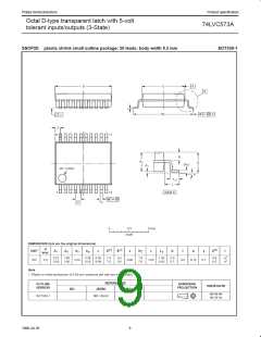
Octal D-type transparent latch with 5-volt
tolerant inputs/outputs (3-State)
74LVC573A
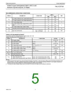
RECOMMENDED OPERATING CONDITIONS
LIMITS
SYMBOL
PARAMETER
CONDITIONS
UNIT
MIN
2.7
1.2
0
MAX
DC supply voltage (for max. speed performance)
DC supply voltage (for low-voltage applications)
DC Input voltage range
3.6
3.6
5.5
V
CC
V
V
V
I
DC output voltage range; output HIGH or LOW
state
0
V
CC
V
O
V
DC output voltage range; output 3-State
0
5.5
T
amb
Operating ambient temperature range in free-air
–40
+85
°C
V
CC
V
CC
= 1.2 to 2.7V
= 2.7 to 3.6V
0
0
20
10
t , t
r
Input rise and fall times
ns/V
f
1
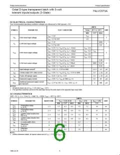
ABSOLUTE MAXIMUM RATINGS
In accordance with the Absolute Maximum Rating System (IEC 134)
Voltages are referenced to GND (ground = 0V)
SYMBOL
PARAMETER
DC supply voltage
CONDITIONS
RATING
UNIT
V
V
CC
I
IK
–0.5 to +6.5
–50
DC input diode current
V t0
mA
V
I
V
I
DC input voltage
Note 2
uV or V t 0
–0.5 to +6.5
"50
I
DC output diode current
V
O
mA
OK
CC
O
DC output voltage; output HIGH or LOW state
DC output voltage; output 3-State
DC output source or sink current
Note 2
Note 2
–0.5 to V +0.5
CC
V
V
O
–0.5 to 6.5
"50
I
O
V
O
= 0 to V
CC
mA
mA
°C
I
, I
DC V or GND current
"100
GND CC
CC
T
stg
Storage temperature range
–65 to +150
Power dissipation per package
– plastic mini-pack (SO)
– plastic shrink mini-pack (SSOP and TSSOP)
P
TOT
above +70°C derate linearly with 8 mW/K
above +60°C derate linearly with 5.5 mW/K
500
500
mW
NOTES:
1. Stresses beyond those listed may cause permanent damage to the device. These are stress ratings only and functional operation of the
device at these or any other conditions beyond those indicated under “recommended operating conditions” is not implied. Exposure to
absolute-maximum-rated conditions for extended periods may affect device reliability.
2. The input and output voltage ratings may be exceeded if the input and output current ratings are observed.
5
1998 Jul 29

 NXP [ NXP ]