Philips Semiconductors
Product specification
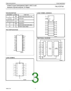
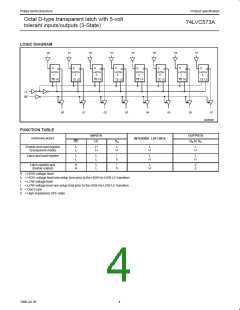
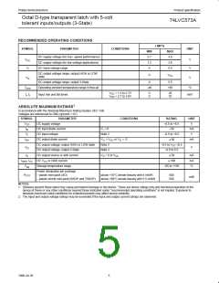
Octal D-type transparent latch with 5-volt
tolerant inputs/outputs (3-State)
74LVC573A
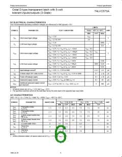
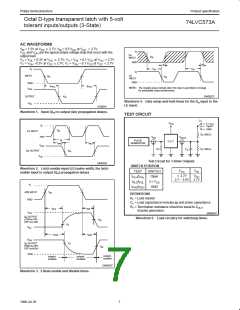
AC WAVEFORMS
V
V
= 1.5V at V w 2.7V; V = 0.5 V at V t 2.7V.
M
CC M CC CC
V
I
and V are the typical output voltage drop that occur with the
OL
OH
Dn
INPUT
output load.
V
M
t
V
X
V
Y
= V + 0.3V at V w 2.7V; V = V + 0.1 V at V t2.7V
OL CC X OL CC CC
GND
= V –0.3V at V w2.7V; V = V – 0.1 V at V t2.7V
OH
CC
Y
OH
CC
CC
th
th
t
V
I
SU
SU
V
I
INPUT
GND
LE
INPUT
V
M
t
V
M
GND
t
PHL
PLH
NOTE: The shaded areas indicate when the input is permitted to change
V
OH
for predictable output performance.
OUTPUT
V
M
SW00073
Waveform 4. Data setup and hold times for the D input to the
LE input.
n
V
OL
SY00041
Waveform 1. Input (D ) to output (Qn) propagation delays.
n
TEST CIRCUIT
S
1
V
CC
2<V
CC
Open
GND
V
I
V
M
LE INPUT
R =500 Ω
L
GND
V
V
OUT
IN
t
w
PULSE
GENERATOR
D.U.T.
t
t
PLH
PHL
V
OH
R =500 Ω
L
R
C
T
L
V
Qn OUTPUT
M
V
OL
Test Circuit for 3-State Outputs
SWITCH POSITION
SA00388
Waveform 2. Latch enable input (LE) pulse width, the latch
enable input to output (Q ) propagation delays
V
V
IN
TEST
SWITCH
Open
CC
n
t 2.7V
2.7 – 3.6V 2.7V
V
CC
t
/t
PLH PHL
t
/t
2<V
CC
PLZ PZL
V
I
t
/t
GND
PHZ PZH
V
nOE INPUT
GND
M
DEFINITIONS
R = Load resistor
L
C = Load capacitance includes jig and probe capacitance
L
R = Termination resistance should be equal to Z
T
OUT
t
t
PZL
PLZ
of pulse generators.
V
CC
SW00047
Q
OUTPUT
n
Waveform 5. Load circuitry for switching times.
LOW-to-OFF
OFF-to-LOW
V
M
V
X
V
OL
t
t
PZH
PHZ
V
OH
Q
n
OUTPUT
V
Y
HIGH-to-OFF
OFF-to-HIGH
V
M
GND
outputs
enabled
outputs
enabled
outputs
disabled
SW00207
Waveform 3. 3-State enable and disable times.
7
1998 Jul 29

 NXP [ NXP ]