Philips Semiconductors
Product specification
Octal D-type transparent latch with 5-volt
tolerant inputs/outputs (3-State)
74LVC573A
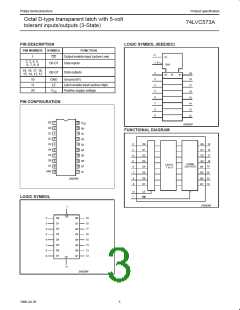
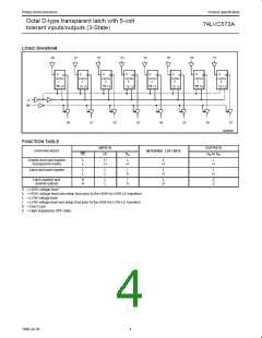
The 74LVC573A is an octal D-type transparent latch featuring
separate D-type inputs for each latch and 3-State outputs for
bus-oriented applications. A latch enable (LE) input and an output
enable (OE) input are common to all internal latches.
FEATURES
• 5-volt tolerant inputs/outputs, for interfacing with 5-volt logic
• Supply voltage range of 2.7V to 3.6V
• Complies with JEDEC standard no. 8-1A
• Inputs accept voltages up to 5.5V
• CMOS low power consumption
• Direct interface with TTL levels
• High impedance when V = 0V
The ’573A’ consists of eight D-type transparent latches with 3-State
true outputs. When LE is HIGH, data at the D inputs enters the
n
latches. In this condition, the latches are transparent, i.e. a latch
output will change each time its corresponding D-input changes.
When LE is LOW, the latches store the information that was present
at the D-inputs one setup time preceding the HIGH-to-LOW
transition of LE. When OE is LOW, the contents of the eight latches
are available at the outputs. When OE is HIGH, the outputs go to the
high impedance OFF-state. Operation of the OE input does not
affect the state of the latches.
CC
• Flow-through pin-out architecture
DESCRIPTION
The ’573A’ is functionally identical to the ’373A’, but the ’373A’ has a
different pin arrangement.
The 74LVC573A is a high-performance, low-power, low-voltage,
Si-gate CMOS device, superior to most advanced CMOS
compatible TTL families.
Inputs can be driven from either 3.3V or 5V devices. In 3-State
operation, outputs can handle 5V. This feature allows the use of
these devices as translators in a mixed 3.3V/5V environment.
QUICK REFERENCE DATA
SYMBOL
PARAMETER
CONDITIONS
TYPICAL
UNIT
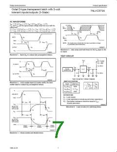
Propagation delay
D to Q
C = 50pF
L
t
/t
ns
PHL PLH
V
CC
= 3.3V
4.3
4.6
n
n;
LE to Q
n
C
C
Input capacitance
Power dissipation capacitance per latch Notes 1 and 2
5.0
20
pF
pF
I
PD
NOTE:
1. C is used to determine the dynamic power dissipation (P in mW):
PD
D
2
2
P
= C x V
x f + S (C x V
x f ) where:
D
PD
CC
i
L
CC o
f = input frequency in MHz; C = output load capacity in pF;
i
L
f = output frequency in MHz; V = supply voltage in V;
o
CC
2
S (C x V
x f ) = sum of outputs.
L
CC
o
2. The condition is V = GND to V
I
CC
ORDERING INFORMATION
TEMPERATURE
RANGE
OUTSIDE
NORTH AMERICA
PACKAGES
NORTH AMERICA
PKG. DWG. #
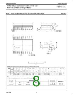
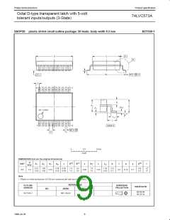
20-Pin Plastic Shrink Small Outline (SO)
–40°C to +85°C
–40°C to +85°C
–40°C to +85°C
74LVC573A D
74LVC573A DB
74LVC573A PW
74LVC573A D
74LVC573A DB
7LVC573APW DH
SOT163-1
SOT339-1
SOT360-1
20-Pin Plastic Shrink Small Outline (SSOP) Type II
20-Pin Plastic Thin Shrink Small Outline (TSSOP) Type I
2
1998 Jul 29
853-1862 19804

 NXP [ NXP ]