ISP1160
Embedded USB Host Controller
Philips Semiconductors
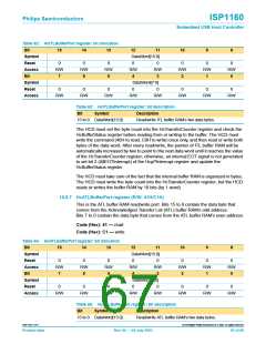
Table 62: HcITLBufferPort register: bit allocation
Bit
15
14
13
12
11
10
9
8
Symbol
Reset
Access
Bit
DataWord[15:8]
0
R/W
7
0
R/W
6
0
R/W
5
0
R/W
4
0
R/W
3
0
R/W
2
0
R/W
1
0
R/W
0
Symbol
Reset
Access
DataWord[7:0]
0
0
0
0
0
0
0
0
R/W
R/W
R/W
R/W
R/W
R/W
R/W
R/W
Table 63: HcITLBufferPort register: bit description
Bit Symbol Description
15 to 0 DataWord[15:0] Read/write ITL buffer RAM’s two data bytes.
The HCD must set the byte count into the HcTransferCounter register and check the
HcBufferStatus register before reading from or writing to the buffer. The HCD must
write the command (40H to read, C0H to write) once only, and then read or write both
bytes of the data word. After every read/write, the pointer of ITL buffer RAM will be
automatically increased by two to point to the next data word until it reaches the value
of the HcTransferCounter register; otherwise, an internal EOT signal is not generated
to set bit 2 (AllEOTInterrupt) of the HcµPInterrupt register and update the
HcBufferStatus register.
The HCD must take care of the fact that the internal buffer RAM is organized in bytes.
The HCD must write the byte count into the HcTransferCounter register, but the HCD
reads or writes the buffer RAM by 16 bits (by 1 word).
10.6.7 HcATLBufferPort register (R/W: 41H/C1H)
This is the ATL buffer RAM read/write port. Bits 15 to 8 contain the data byte that
comes from the Acknowledged Transfer List (ATL) buffer RAM’s odd address.
Bits 7 to 0 contain the data byte that comes from the ATL buffer RAM’s even address.
Code (Hex): 41 — read
Code (Hex): C1 — write
Table 64: HcATLBufferPort register: bit allocation
Bit
15
14
13
12
11
10
9
8
Symbol
Reset
Access
Bit
DataWord[15:8]
0
R/W
7
0
R/W
6
0
R/W
5
0
R/W
4
0
R/W
3
0
R/W
2
0
R/W
1
0
R/W
0
Symbol
Reset
Access
DataWord[7:0]
0
0
0
0
0
0
0
0
R/W
R/W
R/W
R/W
R/W
R/W
R/W
R/W
Table 65: HcATLBufferPort register: bit description
Bit Symbol Description
15 to 0 DataWord[15:0] Read/write ATL buffer RAM’s two data bytes.
9397 750 11371
© Koninklijke Philips Electronics N.V. 2003. All rights reserved.
Product data
Rev. 04 — 04 July 2003
67 of 88

 NXP [ NXP ]