ISP1160
Embedded USB Host Controller
Philips Semiconductors
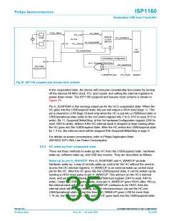
Wake-up by pin CS_N (software wake-up): During the USBSuspend state, an
external microprocessor issues a chip select signal through pin CS_N to the
ISP1160. This method of access to the ISP1160 internal registers is a software
wake-up.
Wake-up by USB devices: For the USB bus resume, a USB device attached to the
root hub port issues a resume signal to the HC through the USB bus, switching the
HC from the USBSuspend state to the USBResume state. This will also set
bit ResumeDetected of the HcInterruptStatus register (03H to read, 83H to write).
No matter which method is used to wake up the HC from the USBSuspend state, the
corresponding interrupt bits must be enabled before the HC goes into the
USBSuspend state so that the microprocessor can receive the correct interrupt
request to wake up the HC.
10. HC registers
The HC contains a set of on-chip control registers. These registers can be read or
written by the Host Controller Driver (HCD). The Control and Status register sets,
Frame Counter register sets, and Root Hub register sets are grouped under the
category of HC Operational registers (32 bits). These operational registers are made
compatible to OpenHCI (Host Controller Interface) operational registers. This allows
the OpenHCI HCD to be easily ported to the ISP1160.
Reserved bits may be defined in future releases of this specification. To ensure
interoperability, the HCD must not assume that a reserved field contains logic 0.
Furthermore, the HCD must always preserve the values of the reserved field. When a
R/W register is modified, the HCD must first read the register, modify the bits desired,
and then write the register with the reserved bits still containing the original value.
Alternatively, the HCD can maintain an in-memory copy of previously written values
that can be modified and then written to the HC register. When a ‘write to set’ or ‘clear
the register’ is performed, bits written to reserved fields must be logic 0.
As shown in Table 7, the addresses (the commands for reading registers) of these
32-bit operational registers are similar to the offsets defined in the OHCI specification
with the addresses being equal to offset divided by 4.
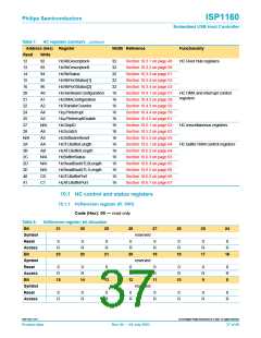
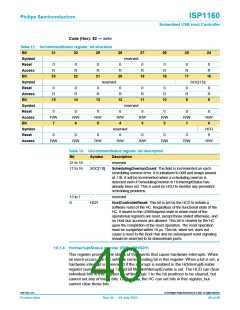
Table 7:
HC registers summary
Address (Hex) Register
Width Reference
Functionality
Read
00
Write
N/A
81
HcRevision
32
32
32
32
32
32
32
32
32
32
Section 10.1.1 on page 37
HC control and status registers
01
HcControl
Section 10.1.2 on page 38
Section 10.1.3 on page 39
Section 10.1.4 on page 40
Section 10.1.5 on page 42
Section 10.1.6 on page 43
Section 10.2.1 on page 44
Section 10.2.2 on page 45
Section 10.2.3 on page 46
Section 10.2.4 on page 47
02
82
HcCommandStatus
HcInterruptStatus
HcInterruptEnable
HcInterruptDisable
HcFmInterval
03
83
04
84
05
85
0D
0E
0F
11
8D
N/A
N/A
91
HC frame counter registers
HcFmRemaining
HcFmNumber
HcLSThreshold
9397 750 11371
© Koninklijke Philips Electronics N.V. 2003. All rights reserved.
Product data
Rev. 04 — 04 July 2003
36 of 88

 NXP [ NXP ]