HEF4051B
NXP Semiconductors
8-channel analog multiplexer/demultiplexer
10.2 ON resistance
Table 7.
ON resistance
Tamb = 25 C; ISW = 200 A; VSS = VEE = 0 V.
Symbol Parameter
Conditions
VI = 0 V to VDD VEE
see Figure 11 and Figure 12
VDD VEE Typ
Max
2500
245
175
340
160
115
365
200
155
-
Unit
RON(peak) ON resistance (peak)
;
5 V
350
80
60
115
50
40
120
65
50
25
10
5
10 V
15 V
RON(rail)
ON resistance (rail)
VI = 0 V; see Figure 11 and Figure 12 5 V
10 V
15 V
5 V
VI = VDD VEE
;
see Figure 11 and Figure 12
10 V
15 V
5 V
RON
ON resistance mismatch
between channels
VI = 0 V to VDD VEE; see Figure 11
10 V
15 V
-
-
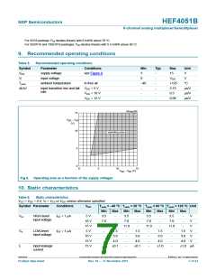
10.2.1 ON resistance waveform and test circuit
V
V
V
SW
DD
S1 to S3
V
or V
DD
SS
Z
E
Yn
V
= V
EE
SS
V
SS
I
V
SW
I
001aak512
RON = VSW / ISW
.
Fig 11. Test circuit for measuring RON
HEF4051B
All information provided in this document is subject to legal disclaimers.
© NXP B.V. 2011. All rights reserved.
Product data sheet
Rev. 10 — 17 November 2011
9 of 23

 NXP [ NXP ]