HEF4051B
NXP Semiconductors
8-channel analog multiplexer/demultiplexer
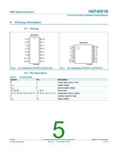
7. Functional description
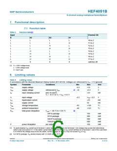
7.1 Function table
Table 3.
Function table[1]
Input
Channel ON
E
L
L
L
L
L
L
L
L
H
S3
L
S2
L
S1
L
Y0 to Z
Y1 to Z
Y2 to Z
Y3 to Z
Y4 to Z
Y5 to Z
Y6 to Z
Y7 to Z
switches off
L
L
H
L
L
H
H
L
L
H
L
H
H
H
H
X
L
H
L
H
H
X
H
X
[1] H = HIGH voltage level;
L = LOW voltage level;
X = don’t care.
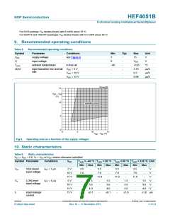
8. Limiting values
Table 4.
Limiting values
In accordance with the Absolute Maximum Rating System (IEC 60134). Voltages are referenced to VSS = 0 V (ground).
Symbol
VDD
Parameter
Conditions
Min
0.5
18
-
Max
+18
+0.5
10
Unit
V
supply voltage
supply voltage
input clamping current
[1]
VEE
referenced to VDD
V
IIK
pins Sn and E;
mA
VI < 0.5 V or VI > VDD + 0.5 V
VI
input voltage
0.5
-
VDD + 0.5
10
V
II/O
input/output current
supply current
mA
mA
C
C
IDD
Tstg
Tamb
Ptot
-
50
storage temperature
ambient temperature
total power dissipation
65
40
+150
+125
[2]
Tamb = 40 C to +125 C
DIP16 package
-
-
-
-
-
750
500
500
500
100
mW
mW
mW
mW
mW
SO16 package
SSOP16 package
TSSOP16 package
per output
P
power dissipation
[1] To avoid drawing VDD current out of terminal Z, when switch current flows into terminals Y, the voltage drop across the bidirectional
switch must not exceed 0.4 V. If the switch current flows into terminal Z, no VDD current will flow out of terminals Y, and in this case there
is no limit for the voltage drop across the switch, but the voltages at Y and Z may not exceed VDD or VEE
.
[2] For DIP16 package: Ptot derates linearly with 12 mW/K above 70 C.
HEF4051B
All information provided in this document is subject to legal disclaimers.
© NXP B.V. 2011. All rights reserved.
Product data sheet
Rev. 10 — 17 November 2011
6 of 23

 NXP [ NXP ]