Philips Semiconductors
Preliminary specification
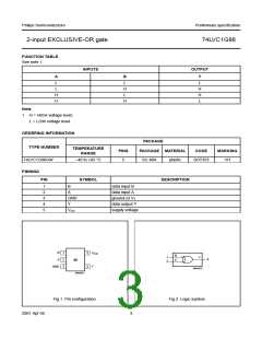
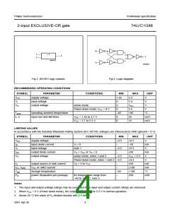
2-input EXCLUSIVE-OR gate
74LVC1G86
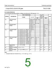
AC CHARACTERISTICS
GND = 0 V; tr = tf ≤ 2.0 ns.
TEST CONDITIONS
WAVEFORMS VCC (V)
Tamb (°C)
SYMBOL
PARAMETER
−40 to +85
UNIT
MIN.
TYP.(1)
MAX.
9.9
t
PHL/tPLH propagation delay A and B to Y see Figs 5 and 6 1.65 to 1.95 1.0
3.7
2.5
2.8
2.3
1.9
ns
2.3 to 2.7
2.7
0.5
0.5
0.5
0.5
5.5
5.8
5.0
4.0
ns
ns
ns
ns
3.0 to 3.6
4.5 to 5.5
Note
1. All typical values are measured at Tamb = 25 °C.
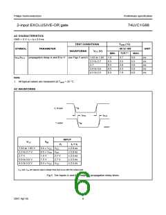
AC WAVEFORMS
handbook, halfpage
A, B input
V
M
t
t
PHL
PLH
V
Y output
M
MNA041
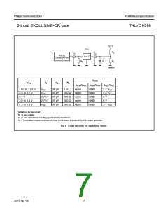
INPUT
VCC
VM
VI
tr = tf
1.65 to 1.95 V
2.3 to 2.7 V
2.7 V
0.5 × VCC VCC
0.5 × VCC VCC
≤ 2.0 ns
≤ 2.0 ns
≤ 2.5 ns
≤ 2.5 ns
≤ 2.5 ns
1.5 V
1.5 V
2.7 V
2.7 V
3.0 to 3.6 V
4.5 to 5.5 V
0.5 × VCC VCC
VOL and VOH are typical output voltage drop that occur with the output load.
Fig.5 The inputs A and B to output Y propagation delay times.
2001 Apr 06
6

 NXP [ NXP ]