Philips Semiconductors
Preliminary specification
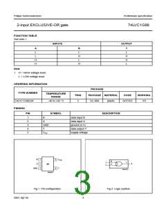
2-input EXCLUSIVE-OR gate
74LVC1G86
FEATURES
DESCRIPTION
• Wide supply voltage range from 1.65 to 5.5 V
• High noise immunity
The 74LVC1G86 is a high-performance, low-power,
low-voltage, Si-gate CMOS device, superior to most
advanced CMOS compatible TTL families.
• Complies with JEDEC standard:
– JESD8-7 (1.65 to 1.95 V)
Inputs can be driven from either 3.3 or 5 V devices. These
features allow the use of these devices in a mixed
3.3 and 5 V environment.
– JESD8-5 (2.3 to 2.7 V)
– JESD8B/JESD36 (2.7 to 3.6 V).
• ±24 mA output drive (VCC = 3.0 V)
• CMOS low power consumption
• Latch-up performance ≤250 mA
• Direct interface with TTL levels
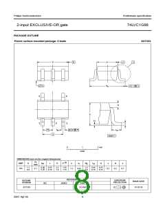
• SOT353 package.
This device is fully specified for partial power-down
applications using Ioff. The Ioff circuitry disables the output,
preventing the damaging backflow current through the
device when it is powered down.
The 74LVC1G86 provides the 2-input EXCLUSIVE-OR
function.
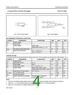
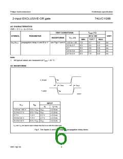
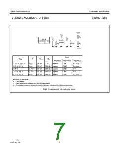
QUICK REFERENCE DATA
GND = 0 V; Tamb = 25 °C; tr = tf ≤ 2.5 ns.
SYMBOL
tPHL/tPLH
PARAMETER
CONDITIONS
TYPICAL
UNIT
ns
propagation delay A and B to Y
VCC = 1.8 V; CL = 30 pF; RL = 1 kΩ
3.7
2.5
2.3
1.9
5
V
V
V
CC = 2.5 V; CL = 30 pF; RL = 500 Ω
CC = 3.3 V; CL = 50 pF; RL = 500 Ω
CC = 5.0 V; CL = 50 pF; RL = 500 Ω
ns
ns
ns
pF
pF
CI
input capacitance
CPD
power dissipation capacitance per notes 1 and 2
buffer
25
Notes
1. CPD is used to determine the dynamic power dissipation (PD in µW).
PD = CPD × VCC2 × fi + (CL × VCC2 × fo) where:
fi = input frequency in MHz;
fo = output frequency in MHz;
CL = output load capacitance in pF;
VCC = supply voltage in Volts.
2. The condition is VI = GND to VCC
.
2001 Apr 06
2

 NXP [ NXP ]