Philips Semiconductors
Preliminary specification
2-input EXCLUSIVE-OR gate
74LVC1G86
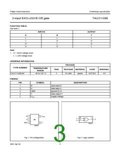
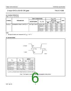
handbook, halfpage
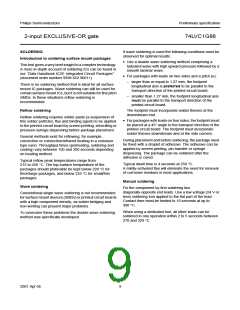
B
handbook, halfpage
1
2
= 1
4
Y
MNA039
A
MNA040
Fig.3 IEE/IEC logic symbol.
Fig.4 Logic diagram.
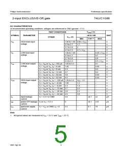
RECOMMENDED OPERATING CONDITIONS
SYMBOL
VCC
PARAMETER
supply voltage
CONDITIONS
MIN.
1.65
MAX.
UNIT
5.5
5.5
V
V
V
V
VI
input voltage
0
VO
output voltage
active mode
0
VCC
5.5
+85
20
Power-down mode; VCC = 0 V
0
Tamb
tr, tf
operating ambient temperature
input rise and fall times
−40
0
°C
VCC = 1.65 to 2.7 V
ns/V
ns/V
V
CC = 2.7 to 5.5 V
0
10
LIMITING VALUES
In accordance with the Absolute Maximum Rating System (IEC 60134); voltages are referenced to GND (ground = 0 V).
SYMBOL PARAMETER CONDITIONS MIN. MAX. UNIT
VCC supply voltage −0.5 +6.5
V
IIK
input diode current
input voltage
VI < 0
note 1
−
−50
mA
V
VI
−0.5
−
+6.5
±50
IOK
VO
output diode current
output voltage
VO > VCC or VO < 0
mA
V
active mode; notes 1 and 2
−0.5
VCC + 0.5
+6.5
±50
Power-down mode; notes 1 and 2 −0.5
V
IO
output source or sink current
VCC or GND current
VO = 0 to VCC
−
mA
mA
°C
mW
ICC, IGND
−
±100
+150
200
Tstg
PD
storage temperature
−65
−
power dissipation per package
for temperature range from
−40 to +85 °C; note 3
Notes
1. The input and output voltage ratings may be exceeded if the input and output current ratings are observed.
2. When VCC = 0 V (Power-down mode), the output voltage can be 5.5 V in normal operation.
3. Above 55 °C the value of PD derates linearly with 2.5 mW/K.
2001 Apr 06
4

 NXP [ NXP ]