74HC132; 74HCT132
NXP Semiconductors
Quad 2-input NAND Schmitt trigger
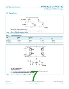
Table 9.
Type
Test data
Input
VI
Load
Test
tr, tf
CL
74HC132
VCC
3.0 V
6.0 ns
6.0 ns
15 pF, 50 pF
15 pF, 50 pF
tPLH, tPHL
tPLH, tPHL
74HCT132
13. Transfer characteristics
Table 10. Transfer characteristics
At recommended operating conditions; voltages are referenced to GND (ground = 0 V); see Figure 7 and Figure 8.
Symbol Parameter
Conditions
Tamb = 25 C
Tamb = 40 C
to +85 C
Tamb = 40 C
to +125 C
Unit
Min Typ Max
Min
Max
Min
Max
74HC132
VT+
VT
VH
positive-going VCC = 2.0 V
0.7 1.18 1.5
1.7 2.38 3.15
2.1 3.14 4.2
0.3 0.63 1.0
0.9 1.67 2.2
1.2 2.26 3.0
0.2 0.55 1.0
0.4 0.71 1.4
0.6 0.88 1.6
0.7
1.7
2.1
0.3
0.9
1.2
0.2
0.4
0.6
1.5
3.15
4.2
1.0
2.2
3.0
1.0
1.4
1.6
0.7
1.7
2.1
0.3
0.9
1.2
0.2
0.4
0.6
1.5
3.15
4.2
1.0
2.2
3.0
1.0
1.4
1.6
V
V
V
V
V
V
V
V
V
threshold
voltage
VCC = 4.5 V
VCC = 6.0 V
negative-going VCC = 2.0 V
threshold
voltage
VCC = 4.5 V
VCC = 6.0 V
hysteresis
voltage
VCC = 2.0 V
CC = 4.5 V
VCC = 6.0 V
V
74HCT132
VT+
VT
VH
positive-going VCC = 4.5 V
1.2 1.41 1.9
1.4 1.59 2.1
1.2
1.4
1.9
2.1
1.2
1.4
1.9
2.1
V
V
threshold
voltage
VCC = 5.5 V
negative-going VCC = 4.5 V
0.5 0.85 1.2
0.6 0.99 1.4
0.5
0.6
1.2
1.4
0.5
0.6
1.2
1.4
V
V
threshold
voltage
VCC = 5.5 V
hysteresis
voltage
VCC = 4.5 V
VCC = 5.5 V
0.4 0.56
0.4 0.60
-
-
0.4
0.4
-
-
0.4
0.4
-
-
V
V
14. Transfer characteristics waveforms
V
O
V
T+
V
I
V
H
V
T−
V
I
V
V
O
H
V
V
T+
T−
mna207
mna208
Fig 7. Transfer characteristics
Fig 8. Transfer characteristics definitions
74HC_HCT132
All information provided in this document is subject to legal disclaimers.
© NXP B.V. 2012. All rights reserved.
Product data sheet
Rev. 3 — 30 August 2012
8 of 20

 NXP [ NXP ]