74HC132; 74HCT132
NXP Semiconductors
Quad 2-input NAND Schmitt trigger
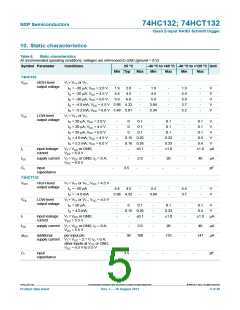
8. Limiting values
Table 4.
Limiting values
In accordance with the Absolute Maximum Rating System (IEC 60134). Voltages are referenced to GND (ground = 0 V).
Symbol
VCC
IIK
Parameter
Conditions
Min
Max
+7
Unit
V
supply voltage
0.5
[1]
[1]
input clamping current
output clamping current
output current
VI < 0.5 V or VI > VCC + 0.5 V
VO < 0.5 V or VO > VCC + 0.5 V
0.5 V < VO < VCC + 0.5 V
-
20
20
25
50
mA
mA
mA
mA
mA
C
IOK
-
IO
-
ICC
supply current
-
IGND
Tstg
Ptot
ground current
50
65
-
storage temperature
total power dissipation
DIP14 package
+150
[2]
-
-
750
500
mW
mW
SO14, and (T)SSOP14
packages
[1] The input and output voltage ratings may be exceeded if the input and output current ratings are observed.
[2] For DIP14 package: Ptot derates linearly with 12 mW/K above 70 C.
For SO14 package: Ptot derates linearly with 8 mW/K above 70 C.
For (T)SSOP14 packages: Ptot derates linearly with 5.5 mW/K above 60 C.
9. Recommended operating conditions
Table 5.
Recommended operating conditions
Voltages are referenced to GND (ground = 0 V)
Symbol Parameter Conditions
74HC132
74HCT132
Unit
Min
2.0
0
Typ
Max
6.0
Min
4.5
0
Typ
Max
5.5
VCC
VI
supply voltage
input voltage
5.0
5.0
V
-
VCC
VCC
+125
-
VCC
VCC
+125
V
VO
output voltage
ambient temperature
0
-
0
-
V
Tamb
40
+25
40
+25
C
74HC_HCT132
All information provided in this document is subject to legal disclaimers.
© NXP B.V. 2012. All rights reserved.
Product data sheet
Rev. 3 — 30 August 2012
4 of 20

 NXP [ NXP ]