74HC132; 74HCT132
NXP Semiconductors
Quad 2-input NAND Schmitt trigger
ꢀꢀꢀꢁꢂꢂꢃꢄꢅꢃ
ꢀꢀꢀꢁꢂꢂꢃꢄꢅꢇ
ꢈꢎꢋ
ꢈꢎꢒ
ꢌꢌ
ꢄꢑꢍꢅ
ꢈꢎꢋ
ꢁ
ꢁ
ꢌꢌ
ꢄꢑꢍꢅ
ꢈꢎꢇ
ꢈꢎꢇ
ꢆꢎꢐ
ꢆꢎꢏ
ꢆꢎꢉ
ꢆ
ꢆꢎꢐ
ꢆꢎꢏ
ꢆꢎꢉ
ꢆ
ꢆ
ꢈ
ꢇ
ꢉ
ꢊ
ꢋ
ꢆ
ꢈ
ꢇ
ꢉ
ꢊ
ꢋ
ꢏ
ꢀ
ꢃꢄꢀꢅ
ꢁꢂ
ꢀ ꢃꢄꢀꢅ
ꢁꢂ
a. VCC = 4.5 V
b. VCC = 5.5 V
Fig 10. Typical 74HCT132 transfer characteristics
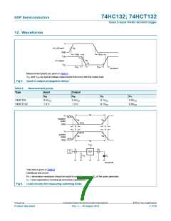
15. Application information
The slow input rise and fall times cause additional power dissipation, this can be
calculated using the following formula:
Padd = fi (tr ICC(AV) + tf ICC(AV)) VCC where:
Padd = additional power dissipation (W);
fi = input frequency (MHz);
tr = rise time (ns); 10 % to 90 %;
tf = fall time (ns); 90 % to 10 %;
ICC(AV) = average additional supply current (A).
Average ICC(AV) differs with positive or negative input transitions, as shown in Figure 11
and Figure 12.
An example of a relaxation circuit using the 74HC132; 74HCT132 is shown in Figure 13.
74HC_HCT132
All information provided in this document is subject to legal disclaimers.
© NXP B.V. 2012. All rights reserved.
Product data sheet
Rev. 3 — 30 August 2012
10 of 20

 NXP [ NXP ]