74HC132; 74HCT132
NXP Semiconductors
Quad 2-input NAND Schmitt trigger
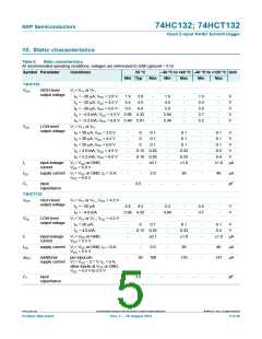
11. Dynamic characteristics
Table 7.
Dynamic characteristics
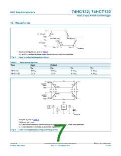
GND = 0 V; CL = 50 pF; for load circuit see Figure 6.
Symbol Parameter
Conditions
25 C
40 C to +125 C Unit
Max Max
(85 C) (125 C)
Min
Typ
Max
74HC132
[1]
tpd
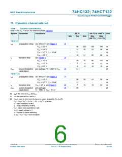
propagation delay nA, nB to nY; see Figure 5
VCC = 2.0 V
-
-
-
-
36
13
11
10
125
25
-
155
31
-
190
38
-
ns
ns
ns
ns
VCC = 4.5 V
VCC = 5.0 V; CL = 15 pF
VCC = 6.0 V
21
26
32
[2]
tt
transition time
see Figure 5
VCC = 2.0 V
VCC = 4.5 V
VCC = 6.0 V
-
-
-
-
19
7
75
15
13
-
95
19
16
-
110
22
19
-
ns
ns
ns
pF
6
[3]
[1]
CPD
power dissipation per package; VI = GND to VCC
capacitance
24
74HCT132
tpd
propagation delay nA, nB to nY; see Figure 5
VCC = 4.5 V
-
-
-
-
20
17
7
33
-
41
-
50
-
ns
ns
ns
pF
VCC = 5.0 V; CL = 15 pF
VCC = 4.5 V; see Figure 5
[2]
[3]
tt
transition time
15
-
19
-
22
-
CPD
power dissipation per package;
capacitance VI = GND to VCC 1.5 V
20
[1] tpd is the same as tPHL and tPLH
.
[2] tt is the same as tTHL and tTLH
.
[3] CPD is used to determine the dynamic power dissipation (PD in W):
PD = CPD VCC2 fi N + (CL VCC2 fo) where:
fi = input frequency in MHz;
fo = output frequency in MHz;
CL = output load capacitance in pF;
VCC = supply voltage in V;
N = number of inputs switching;
(CL VCC2 fo) = sum of outputs.
74HC_HCT132
All information provided in this document is subject to legal disclaimers.
© NXP B.V. 2012. All rights reserved.
Product data sheet
Rev. 3 — 30 August 2012
6 of 20

 NXP [ NXP ]