74HC132; 74HCT132
NXP Semiconductors
Quad 2-input NAND Schmitt trigger
12. Waveforms
V
I
nA, nB input
GND
V
M
t
t
PLH
PHL
V
OH
V
Y
V
nY output
M
V
X
V
OL
t
t
TLH
THL
001aai814
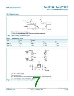
Measurement points are given in Table 8.
VOL and VOH are typical voltage output levels that occur with the output load.
Fig 5. Input to output propagation delays
Table 8.
Type
Measurement points
Input
VM
Output
VM
VX
VY
74HC132
0.5VCC
1.3 V
0.5VCC
1.3 V
0.1VCC
0.1VCC
0.9VCC
0.9VCC
74HCT132
t
W
V
I
90 %
negative
pulse
V
V
V
M
M
10 %
GND
t
t
r
f
t
t
f
r
V
I
90 %
positive
pulse
V
M
M
10 %
GND
t
W
V
CC
V
V
O
I
G
DUT
R
T
C
L
001aah768
Test data is given in Table 9.
Definitions test circuit:
RT = termination resistance should be equal to output impedance Zo of the pulse generator.
CL = load capacitance including jig and probe capacitance.
Fig 6. Load circuitry for measuring switching times
74HC_HCT132
All information provided in this document is subject to legal disclaimers.
© NXP B.V. 2012. All rights reserved.
Product data sheet
Rev. 3 — 30 August 2012
7 of 20

 NXP [ NXP ]