Voltage Regulators
AN8026
■ Application Notes (continued)
[2] Operation descriptions (continued)
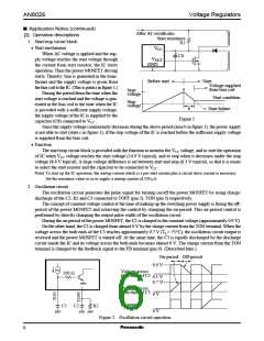
6. Overcurrent protection circuit
The overcurrent of the power supply output is proportional to the value of current flowing in the main switch
in the primary side (the power MOSFET). Taking advantage of the above fact, the overcurrent of the power supply
output is restricted by regulating the upper limit of the pulse current flowing in the main switch to protects the
parts easily damaged by the overcurrent.
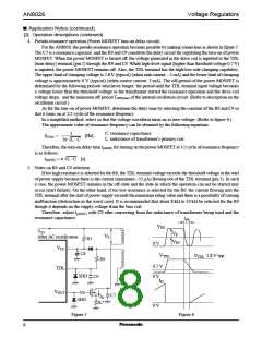
The current flowing in the main switch is detected by monitoring the voltage of both ends of the low resistor
which is connected between the source of power MOSFET and the power supply GND. When the power MOSFET
is turned on and the threshold voltage of CLM (current limit) is detected, the circuit turns off the output and turns
off the power MOSFET to control so as not to allow further current flow. The threshold voltage of CLM is
approximately 0.75 V (typical) under Ta = 25°C with respect to GND. This control is repeated for each cycle. Once
the overcurrent is detected, the off condition is kept during that cycle and it can not be turned on until the next
cycle. The overcurrent detection method described in the above is called "pulse-by-pulse overcurrent detection".
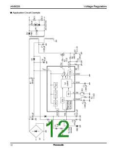
The R6 and C6 in figure 7 construct the filter circuit for removing the noise
generated by the parasitic capacitance equivalently accompanied when turn-
ing on the power MOSFET.
For the earth point, it is recommended that the connection between GND
of the IC and GND of the AC rectifier capacitor should be shortest.
R6
CLM
C6
R7
GND
• Notes on the detection level precision
Figure 7
This overcurrent detection level reflects on the operating current level of the power supply overcurrent
protection. Therefore, if this detection level fluctuates with temperature or dispersion, the operating current level
of the overcurrent protection of power supply itself also fluctuates. Since such level fluctuation means the neces-
sity for an increase in the withstanding capability of used parts and in the worst case it means the cause of
destruction, the accuracy of detection level is increased as much as possible for the AN8026 (approximately
±4%).
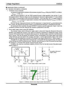
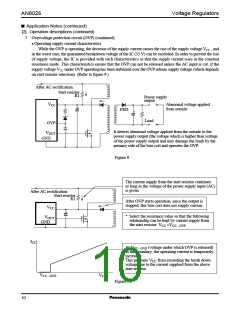
7. Overvoltage protection circuit (OVP)
OVP is an abbreviation of over voltage protection. It refers to a self-diagnosis function, which stops the power
supply to protect the load when the power supply output generates abnormal voltage higher than the normal
output voltage due to failure of the control system or an abnormal voltage applied from the outside. (Refer
to figure 8.)
Basically, it is set to monitor the voltage of supply voltage VCC terminal of the IC. Normally, the VCC voltage
is supplied from the transformer drive coil. Since this voltage is proportional to the secondary side output voltage,
it still operates even when the secondary side output has overvoltage.
1) When the voltage input to the OVP terminal exceeds the threshold voltage (7.9 V typical) as the result of
power supply output abnormality, the protective circuit shuts down the internal reference voltage of the IC to
stop all of the controls and keeps this stop condition.
2) The OVP is released (reset) under the following two conditions:
(1) Setting the OVP terminal voltage at low from outside (lower than approximately 7 V)
(2) Decreasing the supply voltage (VCC < 8.2 V typical: OVP release supply voltage)
When the IC starts its operation, the open bias of approximately 6.5 V is generated in the OVP terminal.
•When the supply voltage becomes lower than the stop voltage,
•When the supply voltage becomes lower than the OVP release voltage,
The discharge circuit is incorporated so that the electric charge which is charged in the capacitor connected to
the OVP terminal can be discharged momentarily for the next re-start.
secondary side output voltage under normal operation VOUT
Vth(OUT)
=
× V7
VCC terminal voltage under normal operation
Vth(OUT) : Secondary side output overvoltage threshold value
th(OVP) : OVP operation threshold value
VZ : Zener voltage (externally attached to OVP terminal)
V7 = Vth(OVP) + VZ
V
9

 PANASONIC [ PANASONIC ]